An Attack Decay Sustain Release (ADSR) is an envelope generator, which is a fancy way of saying it adjusts the volume or other note qualities over time. Each time a note starts, the ADSR outputs a specific voltage sequence that modifies the parameters of the destination module. Both of these circuits control sound qualities, which can be difficult to convey in words. Under Resources is a link to my YouTube video “How to program analog synthesizers” with many audio examples, including how an LFO and ADSR can vary the sound over time.
The LFO
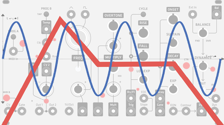
Most LFOs offer several waveforms including square, pulse, triangle, and sawtooth, as shown in Figure 1. A square wave can be changed to a pulse by varying its duty cycle, and a triangle wave can likewise become a sawtooth. A triangle wave is useful for vibrato because it raises and lowers the pitch at the same rate. Adjusting the output voltage of the LFO controls the strength of the effect. A sine wave is more difficult to generate, and when used as a modulator in an LFO it sounds about the same as a triangle wave. So there’s little need to offer a sine wave.

The pulse and sawtooth waves can also be biased in the opposite direction, so the pulse is positive for longer than negative, or the sawtooth rises more slowly than it descends. As audio, such waveform pairs would sound the same because they have the same harmonic content. But as control voltages for pitch, the sawtooth pair would sound like two different sirens — slow up and fast down, or vice versa. Using a pulse for volume would make either the loud part or soft part longer or shorter. Using a square or pulse wave to shift the frequency will toggle between two note pitches (e.g., a European police siren) rather than glide smoothly from one to the other as happens with a triangle or sawtooth wave.
Earlier I mentioned creating AM and FM sidebands. When the volume or frequency of a musical note is modulated at an audible rate, additional frequencies are created related to the sum and the difference of the source and modulating frequencies. Depending on the frequency ratios, depth of modulation, and harmonic content of the source and modulating frequencies, this can create a variety of interesting timbres from warm tones to harsh metallic clanging effects. AM and FM are a staple of digital synthesizers, but they can be created just as easily using analog circuitry. For fun, the Project Files found in the Supplementary Materials section of the audioXpress website has links for two pairs of 2-second .wav files I created using both AM and FM to modulate a swept frequency at a fixed rate. One pair modulates a swept sine wave and the other sweeps a sawtooth wave. The source waves sweep from 400Hz to 600Hz while the modulator stays at a constant 80Hz.
The ADSR
ADSR — Attack, Decay, Sustain, and Release — are parameters set by the user via potentiometer knobs on the front panel. Some synthesizers have additional parameters, such as an initial delay before the ADSR sequence begins, or a second set of attack and decay times that happen after the first pair completes. But most ADSRs offer these four basic parameters. Note that the Attack, Decay, and Release settings control the length of each event, but the Sustain knob controls the sustained voltage level before the final Release.
Figure 2 shows how the output voltage changes over time for a typical ADSR setting, and Figure 3 shows the result as applied to the volume of a 100Hz sine wave. This sequence begins whenever a note is played, whether on a keyboard or, in this case, an electric guitar. When a note starts the ADSR’s output voltage begins to ramp up until it reaches 10V. Of course, 10V is arbitrary based on the synthesizer’s design. Further, the amount an ADSR affects its destination module can be varied by its output amount, or by an input level control at the destination module.
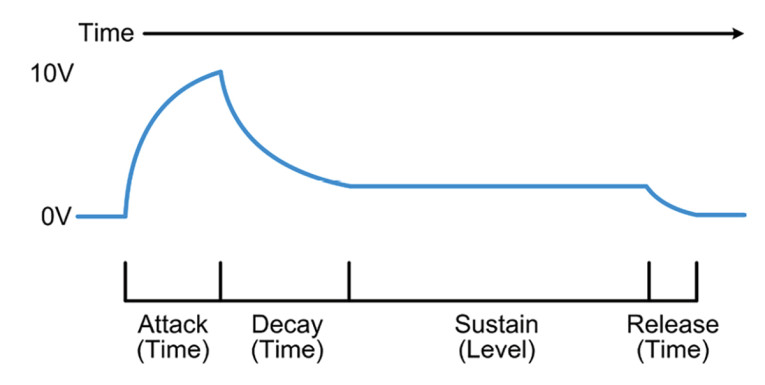

Once the voltage reaches its maximum at a speed set by the Attack time, it begins to fall at a rate set by the Decay control. But rather than decay back to zero volts, it instead drops down to the Sustain level. When used to control volume, this lets you create a short note burst for greater articulation, then settle to a lower volume for the duration of the note to better blend with the rest of the music. This is a common playing technique for brass and other acoustic instruments. When the player stops the note, the volume falls back to zero at a rate determined by the Release setting.
LFO Circuit Details
As with my previous articles in this series, the circuits shown here were developed using the freeware LTspice virtual circuit simulator. This program from IC maker Analog Devices offers a fully stocked parts bin with a virtual oscilloscope, Bode and FFT frequency analysis, signal generators, and more. You draw the schematic, then click Run to watch it work. Once the circuit performs as expected you can buy the parts and build it for real. This is much faster and easier — and less expensive! — than using a breadboard, especially with a large project such as this synthesizer. And you’ll never blow up an expensive component accidentally. Links to the program’s download page and support forum are under Resources.
Before diving into the LFO circuit it will be useful to introduce the concept of hysteresis. This applies a controlled amount of positive feedback to preserve a system’s state, and in practice means “Don’t turn off the furnace until you get slightly above the temperature I set.” Hysteresis resists change by requiring a condition to be exceeded, not just met, before the change finally occurs. Without hysteresis — typically a bi-metal coil spring attached to a switch and magnet — your furnace or air conditioner would cycle on and off every few seconds as the temperature varied ever so slightly above and below the thermostat setting.
Figure 4 shows the schematic for the LFO circuit. Op-amp U1 is configured as an integrator that charges capacitor C1 up then down over time, and that provides the triangle wave output. The triangle voltage feeds comparator U2 whose output switches from fully positive to fully negative each time the triangle passes through zero volts. This serves as the LFO’s square wave output. However, R1 and R2 implement hysteresis, so the triangle voltage must exceed zero volts in both directions before the comparator’s output flips.
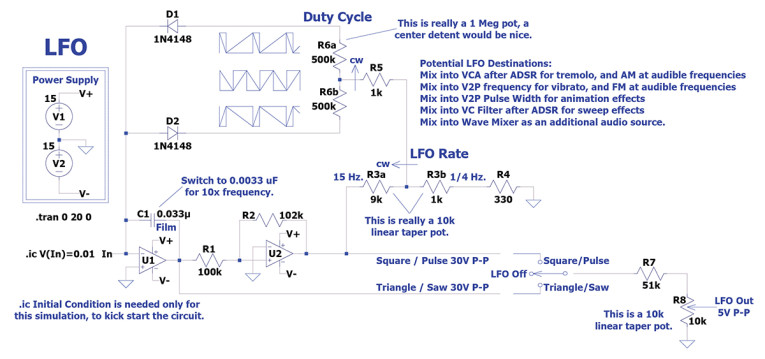
With nearly equal resistor values for R1 and R2, the triangle wave must ramp up almost to the +15V power supply before it overcomes the opposing -15V from the comparator’s output. That finally forces its own plus input past zero volts (ground) at the minus input. When that happens the comparator’s output flips polarity and capacitor C1 begins ramping in the opposite direction. Without hysteresis the triangle’s output voltage would be extremely small and at a very high frequency due to the comparator constantly switching states around zero volts. You can see how this works by reducing R1 while monitoring the output and plus input of U1.
Note that LTspice doesn’t have a potentiometer component. So in both the LFO and the ADSR circuits you’ll see some potentiometers set up as resistor pairs, with separate values for each side of the pot’s variable wiper. For example, R3 in Figure 4 is almost fully counter-clockwise to set a low frequency using 9k + 1k. If you play with the circuit in LTspice, change both resistors so they total the stated value.
Potentiometer R3 controls the amount of current available to charge C1, so that sets the LFO’s frequency. There are also limit resistors R4 and R5 that prevent too much or too little current for the circuit to operate properly. Potentiometer R6 uses a pair of diodes to vary the capacitor’s up and down ramp times independently. The waveform drawings to the left of R6 show how the duty cycle can be varied over a wide range in either direction. It’s not practical for a single knob to control a frequency range much larger than 60-to-1 used here. So the final synthesizer will have a switch to select C1 as either 0.033µF as shown, or 0.0033µF to allow frequencies 10 times higher.
The last LFO item is the LTspice directive .ic, which sets an Initial Condition at any point in a circuit. Due to the vagaries of power supply turn-on voltage, LTspice can’t always know what voltage will appear initially at every node in the circuit. Depending on the values of C1 and R3, without .ic this circuit won’t start to oscillate until several seconds have passed. Forcing 10mV into U1’s minus input begins ramping C1 to kick start the circuit. Note that the label In is not an input to the circuit, but rather the circuit node where LTspice is to insert the initial voltage. You don’t need to name .ic destination nodes, but doing so is good practice because the internal node numbers can change as a circuit is edited. Naming the node guarantees that .ic will always be applied to the correct place.
ADSR Circuit Details
This ADSR was first used in the monster analog synth my friend Leo Taylor and I built in 1970, mentioned in the April 2022 issue of audioXpress. If you have LTspice and run the ADSR.asc file from the Supplementary Materials, you can probe various places in the circuit to better follow the descriptions that follow.
In this guitar synth a Pick Detector (not yet shown) outputs a brief positive pulse every time a note is picked. So the first element in the ADSR is inverter A1 that reverses the polarity to negative as needed by the 555 timer’s Trigger input to start the timing cycle. This trigger pulse also resets the timer, in case a new note is played before the Attack portion of the current note completes. Once triggered the timer starts charging capacitor C4 which, along with potentiometer R3, determines the Attack time. With the 80K and 2.2µF values shown, this is about 220mS. At the end of that period, the timer discharges capacitor C4 back to zero volts to begin another cycle when the next note is played. The remaining segments of the ADSR sequence also depend on C4 remaining at zero volts.
The input trigger also sends a brief pulse through transistors Q3 and Q4 to discharge capacitor C5 (Figure 5). This is the main capacitor that establishes the ADSR’s behavior. A film type is used to increase linearity, and avoid voltage sag due to current leakage during the Sustain portion of the cycle. Although C4 sets the Attack time, C5 follows along because it’s tied to the output side of diode D2, which pulls it up in sync with C4.
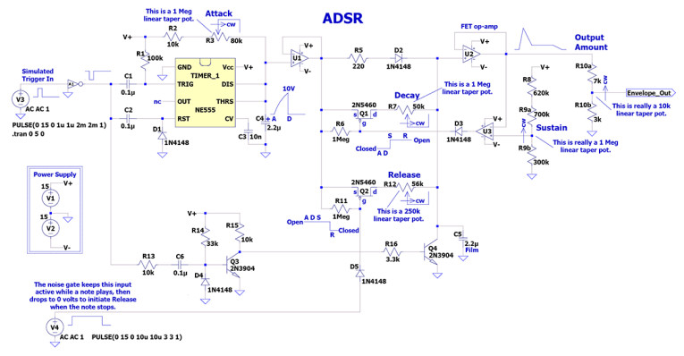
Note the second “digital” input at the lower left that stays high while the incoming note is active. That comes from a noise gate elsewhere in the synthesizer that monitors the incoming notes from the electric guitar. When a note fades completely, or is stopped by the player, the gate shuts down telling the ADSR to begin its final Release phase. Even though the incoming guitar note has ended, the synthesizer’s oscillators continue allowing the note to fade out over the Release time.
Resuming the circuit description, the rising Attack voltage at C4 is buffered by op-amp U1 to isolate C4 from the circuits that follow. That voltage is passed on to the output through another buffer, U2, but through diode D2. With the diode, the Attack cycle can only raise the output, but not drag it back down to zero volts when the timer finishes and resets C4. Instead, FETs Q1 and Q2 serve as switches that pull C5 back down to zero volts, first at the Decay rate, then later at the Release rate. In this case, zero volts is the output of U1 rather than an actual ground connection. An FET op-amp is used for U2 because its very small input bias current avoids draining C5 during the Sustain portion of the cycle.
When a FET is used as a switch, the voltage between its source and gate determines the switch state. The 1M resistors R6 and R13 tie each FET’s gate to its source to hold the switches in the closed state (conducting) until the gate is forced positive relative to the source. P-channel junction FETs, such as the 2N5460 used here, have a resistance of about 300Ω when closed. Then when the gate is at least 3V to 4V more positive than the source the switch becomes an open circuit. Note that diodes in series with each FET gate let the comparator and noise gate pull the FET gates in the positive direction only, to force them open.
When the Attack portion completes, the output of U1 returns to zero, which begins to discharge C5 through FET switch Q1. This switch remains closed until C5 has drained down to the Sustain voltage. At that point comparator U3 flips positive and opens switch Q1, so the capacitor continues to hold its charge at that voltage. When the note finally ends, switch Q2 is closed by the noise gate, which discharges C5 the rest of the way down to zero. Again, the output of U1 is the zero volt discharge path instead of ground.
That’s All, Folks
I hope readers enjoyed seeing these circuits as much as I enjoyed describing them. As “digital” and DSP have overtaken the world of audio, it’s refreshing to know that there’s still room for purely analog designs. Op-amps especially are amazingly powerful and versatile circuit building blocks, and they’re still at the core of many audio products including microphone and phono preamps, active crossovers, and of course analog synthesizers!
Project Files
To download additional material and files, including the Sample & Hold LTspice file, visit
http://audioxpress.com/page/audioXpress-Supplementary-Material.html
Recources
LTspice, www.analog.com/en/design-center/design-tools-and-calculators/ltspice-simulator.html
LTspice online support forum, https://groups.io/g/LTspice
E. Winer, “How to Program Analog Synthesizers,”
www.youtube.com/watch?v=NMF8F9z7Zr8
This article was originally published in audioXpress, June 2022.
Read the other articles in this Building a Guitar-Controlled Synthesizer series
Part 1 - The Sample and Hold Time Machine
Part 2 - Frequency to Volts and Back
Part 4 - Input Section
Part 5 - VCA and VCF