In this article we pick up the design for the Bel Amp with a folded cascode mirror voltage amplification stage (VAS). In Part 1 (audioXpress, February 2025), Figure 4 shows RL converts the differential current into a voltage. Instead, stage one output current can flow into a folded cascode, in pursuit of the goal of low distortion through current amplification. Figure 8 shows this change.
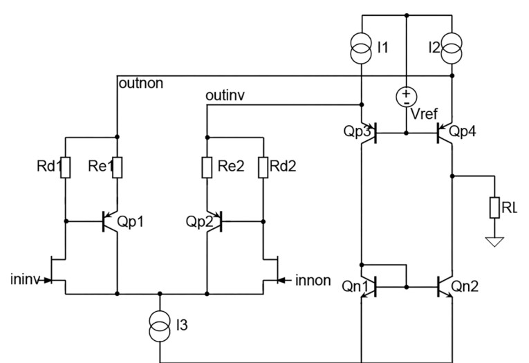
The differential folded cascode is the VAS. It sets the upper voltage of the two CFPs and, by using a shunt voltage regulator, anchors both stages to a voltage referenced to the positive rail. Voltage amplification occurs at the RL node where the differential current signal from stage one is reflected by the cascode into the current mirror of Qn1+Qn2 and multiplied by the impedance at the output node connected to RL.
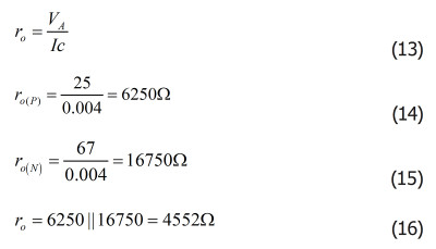
Ignoring RL, small signal output impedance of the voltage amplification stage is set by the parallel combination of ro for Qp4 and Qn2, which are set by their respective Early voltages [10]. BC847C and BC857C were selected for this design due to their high beta (β or hFE) current transfer ratio. As always with engineering there is a trade-off for the high β, where it reduces Early voltage, which in turn reduces overall stage gain. In this case it’s a good compromise because stage gain is plenty high enough. With Early voltages of 25 (PNP) and 67 (NPN) (from their SPICE models) we can calculate the ro value as:
Using the transconductance value from Equation 10 (shown in Part 1) gives voltage gain Av of 51dB with RL=∞:
To see how node voltages are essentially static, let’s examine the internals of Figure 8. The two JFET sources are fixed by their Vgs, nodes outnon and outinv are fixed by Vref + Vbe of Qp3+Qp4. The collector voltage of Qp3 is fixed by Qn1 Vbe. Noise from current source I3 is differentially nulled, noise from Vref is differentially nulled across the current mirror, both positive and negative power supply noise are nulled by differential stage 1 and stage 2.
This gives us a high-quality input stage with high input impedance, fully differential inputs, high gain and fixed voltage at all nodes save one. Later I will show simulation and actual implementation test results of noise and distortion performance.
Adding a Transimpedance Amplifier
RL decreases stage output impedance because it is in parallel with ro and worse, it creates voltage swing across the collector-base of Qp4 and Qn2, potentially adding distortion. By connecting RL to the summing junction of a transimpedance amplifier “transZ”, current becomes voltage while keeping the high impedance node at RL fixed at virtual ground.
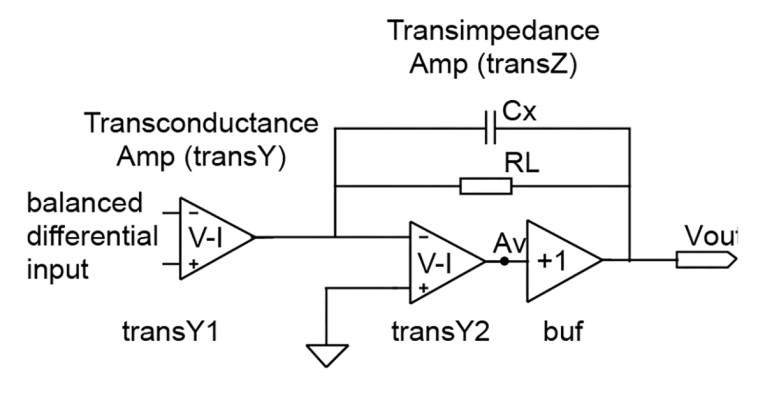
Figure 4 (from Part 1) can become a complete op-amp by adding an output buffer. Figure 9 shows a block diagram with a +1 gain buffer (buf) following transY2, in a closed feedback loop. The combination of transY and transZ gives a two stage non-inverting amplifier (remember the Jim Williams rule mentioned in Part 1) where the first node to have any significant voltage change is the second stage buffer’s input (node labeled Av). Output current from section one is converted to voltage via the feedback resistor around stage two. Terminating the VAS node of transY into the virtual ground of transZ holds transY output at constant voltage, making the node labeled Av in Figure 9 the first node with significant voltage excursion.
Using RL=7.5kΩ reduces calculated gain to 47dB. As a bonus we can put a feedback capacitor Cx in parallel with RL to set the 75µsec (2122Hz) RIAA high-frequency roll-off pole. The high-frequency pole as the first filter point in the RIAA chain improves overload margin by reducing treble amplitude before additional amplification stages [11].
Open Loop with Feedback
Remember the remarks on gain, feedback, and ameliorating distortion with negative feedback? While transY1 in Figure 9 is operated open loop, it does indeed have 26dB local negative feedback for Re=649Ω to reduce input stage distortion. In transZ, the embedded transY2 can also have the same Re, with total forward gain of 67dB (800mV/A times RL=2266Ω) because total gain remains the same whether feedback is global or local or both [12].
And Finally, an Output Buffer
Output unity gain buffers can generate distortion, typically crossover distortion in a Class AB pair, at the transition point when one output driver turns off and another turns on. The design shown in Figure 10 is a diamond buffer modified to source or sink high current while avoiding distortion. QP5.1, QN3.2, QN7.1, and QP6.2 make a standard diamond buffer. M1.1 and M1.2 are a complementary MOSFET pair that are each pre-biased by Vbe of QN7.1 or QP6.2. Then as output current increases from the emitter, it generates additional Vgs across R25 and R26 to turn on the MOSFETs, which supplement the output current from about 5mA up to 80mA. At 80mA, QN7.2 and QP6.1 turn on, stealing drive current from I1 and I2 to limit output current.
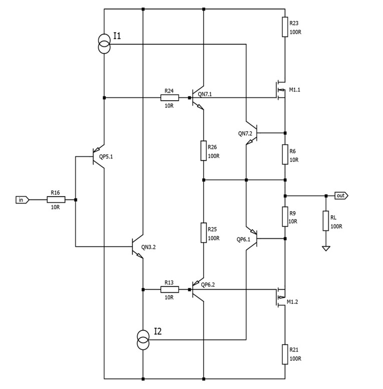
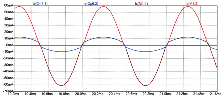
Figure 11 shows simulated output current waveforms for the four transistors, blue are bipolar emitter currents and red are field-effect transistor (FET) source currents. To prevent excess idle current in the MOSFETs, their Vgs turn-on thresholds must be higher than bipolar Vbe, which is almost always the case. The boosted buffer can deliver enough current to drive 100Ω headphones to ±7V and 0.5W and is stable with up to 700pF of cable capacitance.
Performance Simulation and Measurement
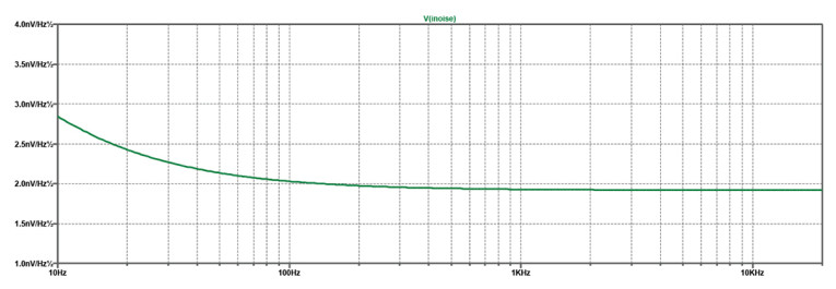
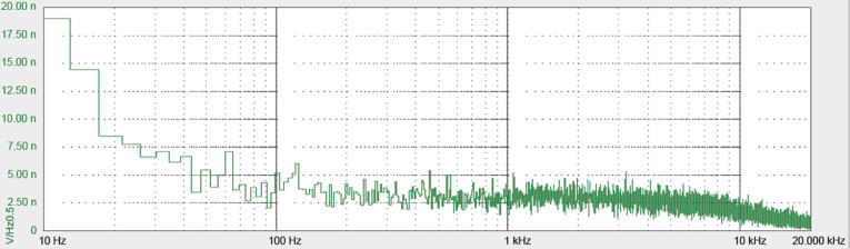
Noise. Input referred noise from an LTSpice simulation looks as one would expect, mostly the same as the LSK389A JFETs. Compare Figure 12 with the datasheet, they are almost identical. The horizontal and vertical axes are configured the same to make it easy. Also, noise may not be included in all the component models used in the simulation. Using functionality in the Handyscope WS5 [13], I created a real-time noise voltage density measurement as seen in Figure 13. Measured noise is higher than the simulation, no surprise. It is still really low, 3nV/√Hz at 1kHz and 350nVrms over the audio bandwidth. The noise at 10-20nV/√Hz below 20Hz is totally inaudible.
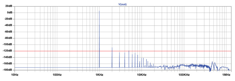
Distortion Simulation. Given perfectly matched transistor pairs and no thermal interaction, a distortion simulation shows very good results. Figure 14 shows a Fast Fourier Transform (FFT) of the total harmonic distortion (THD) data, notice second harmonic is about -110dBV, all others are less.
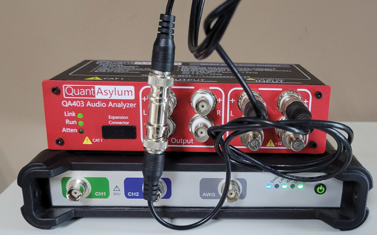
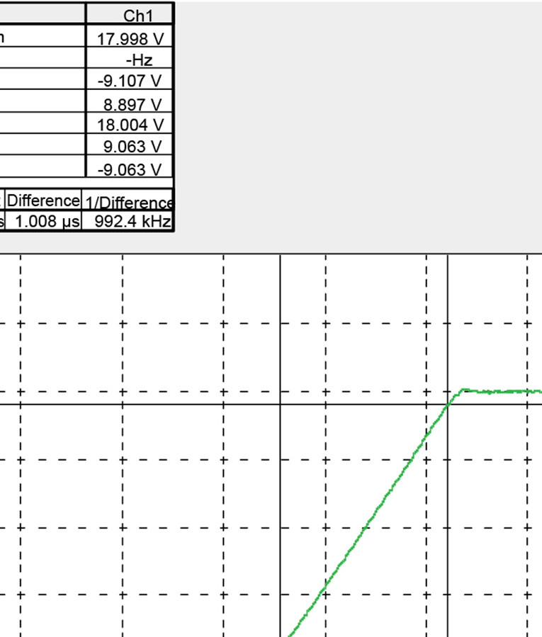
THD Measurement. Measuring harmonic distortion turned out to be more difficult, mostly due to limitations of the equipment. As we are measuring microvolts, anything can be a source of error. The idea is to generate a perfect sine wave, send it through the op-amp and measure it with a perfect analyzer to see if anything changed. If the generated sine wave has any flaws, they will appear in the analyzer, so the first order of business was to test the distortion analyzer, a QuantAsylum QA403. It has two sine sources and two analyzer inputs (actually four of each in differential mode).
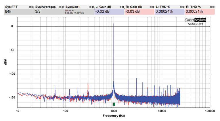
By connecting one sine source to both analyzer inputs as shown in the physical arrangement in Photo 1, we can check if they match. The left source was connected to both analyzer L and R inputs. The test results are shown in Figure 15. Notice the “THD%” values in the upper right with 0.00024% and 0.00021%. This is the baseline measurement limit of this instrument. For the cost, it is very good performance. Turns out it’s really hard to generate or capture a pure sinusoidal wave.
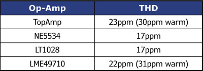
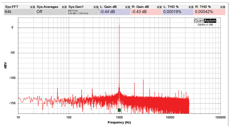
Measured THD shows a second harmonic at -110dB, with the third higher at -103dB, all others below -120dB. The total of DUT is 42ppm, and the difference is 42–19=23ppm, or 0.00023% distortion from the Bel Amp. Plugging other commercially available audiophile grade op amps into the same test fixture shows similar performance, see Table 2. It is notable that DUT temperature can change THD — two were measured quickly then again after a few minutes to warm up and stabilize. THD increased for both after warm-up. This is where integrated circuits may have a (small) edge: due to techniques such as cross-coupled layout, warm-up effects are minimized.
AC Analysis
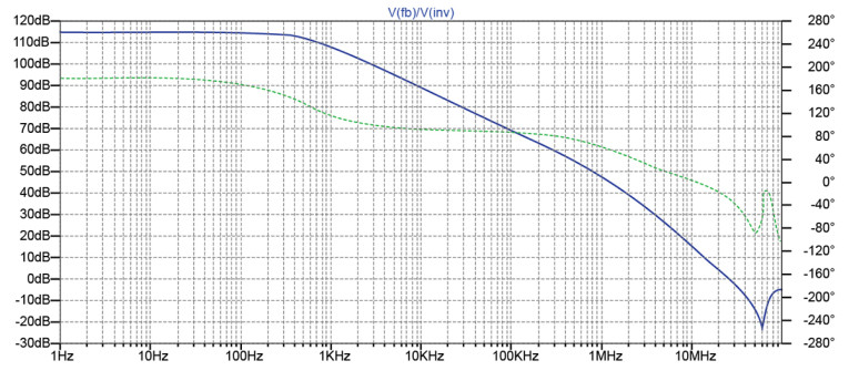
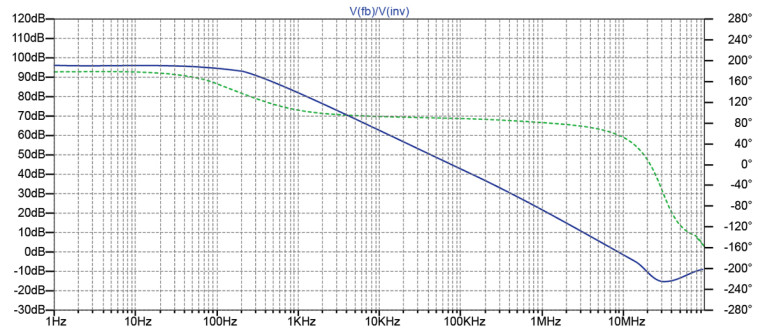
Open Loop Gain Simulation. As discussed earlier, stage 1 has local feedback that can affect the overall gain measurement. To determine total open loop gain, a simulation is done with Re1 and Re2 from Figure 8 set to zero (actually 1e-9R in LTSpice). This gives the theoretical maximum Avol of 115dBV, crossing unity gain at greater than 20MHz as seen in Figure 17. “External” open loop gain with internal local feedback is simulated with Re1 and Re2 = 649Ω and seen in Figure 18. Peak gain decreased to 95dB, with the difference giving the amount of internal local feedback as 20dBV. Unity gain crossover frequency is 9MHz and the phase reversal at 60MHz is gone.
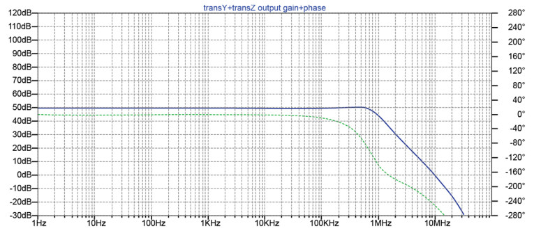
It’s also a worthwhile exercise to simulate the transY+ transZ pair from Figure 9 to allow a direct gain comparison of the combined input between simulation and real circuit, since Avol is a difficult parameter to measure. This is plotted in Figure 19. Gain is just below 50dB, very close to the 51dB from Equation 17 and almost 3dB higher than the value of 47dB calculated using RL=7.5kΩ.
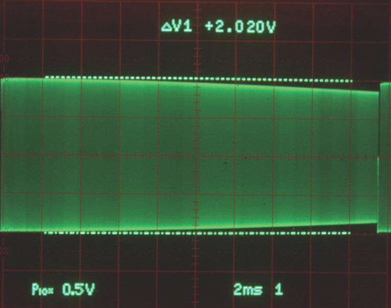
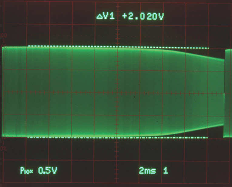
Gain-Bandwidth. The QA403 maximum sample rate is 96kHz, so is not suitable for testing the bandwidth of a high-speed op-amp. I also could not get a good bandwidth spectrum from a Handyscope WS5 so instead opted to use a trusted old 150MHz bandwidth analog scope and see where bandwidth rolls off. The Handyscope does provide a nice sine wave swept linearly from 1kHz to 2MHz (actually specified up to 100MHz! [14]). A 1Vpk wave was driven into the op-amp in unity gain inverting mode, and swept output is shown in Figure 20. The bottom edge shows a slight amplitude increase starting at 1.4MHz. As a sanity check, a LME49710, a NE5534, and a LT1028 were also tested in the same socket (Figures 21-23). The LT1028 has a two-stage VAS with internal pole-zero compensation [15] (similar to OP-07 and other George Erdi designs), which may explain the weirdness above 1.5MHz in that sweep.
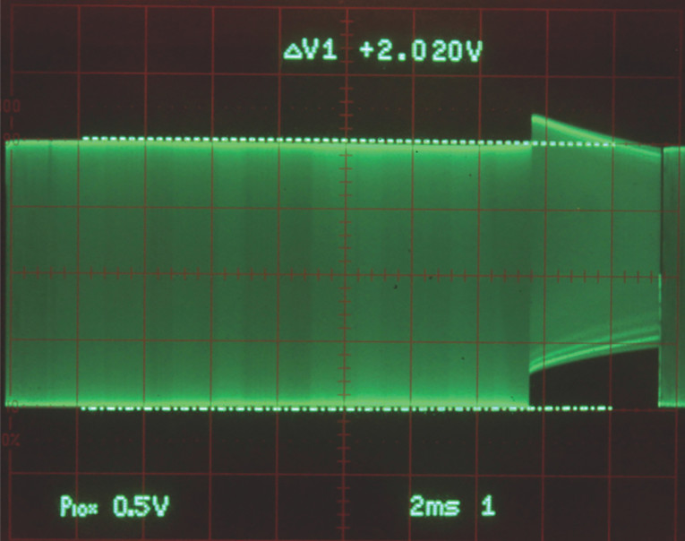
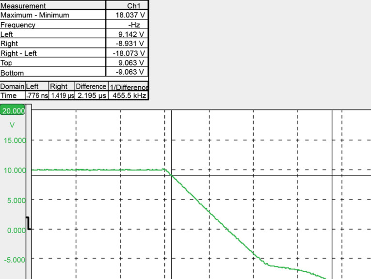
Slew rate. How does the boosted diamond buffer output perform? Clearly it has low distortion. Slew rate is plenty adequate for audio, at 12V/µsec positive and 8V/µsec negative (Figure 24 and Figure 25). Figure 25 has an odd negative settling characteristic. It does not show on a simulation and I’m investigating the cause.
The Bottom Line
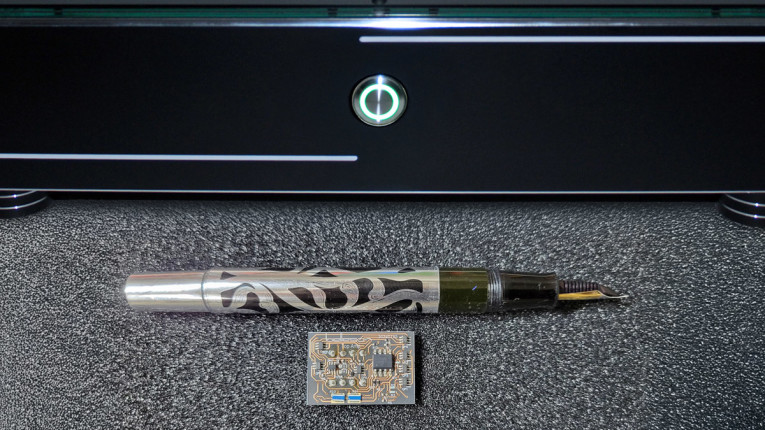
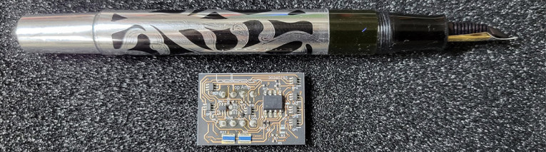
The composite transY+transZ amplifier is great for a phono stage and could be used as a high impedance microphone preamp. Internal resistors can be tweaked to adjust supply current, although there is a balance between least distortion and power dissipation. The measured design draws 32mA from ±16V power supplies, which may be rather high for some applications. We have built a surface mount version of Bel Amp on a 1.8cm × 2.7cm two-layer PCB (Photo 2). We’re happy to have an op-amp design that meets the goals defined in the introduction. aX
References
[10] P. R. Gray and R. G. Meyer, Analysis and Design of Analog Integrated Circuits, p. 36, John Wiley & Sons, 1977.
[11] B. Cordell, “VinylTrak – A full-featured MM/MC phono preamp,” Linear Audio, Volume 4, p. 135, September 2012.
[12] B. Putzeys, “The F-word or, why there is no such thing as too much feedback,”
www.linearaudio.net/index.php/f-word-or-why-there-no-such-thing-too-much-feedback-0
[13] Tiepie Handyscope HS5, www.tiepie.com/en/wifi-oscilloscope/wifiscope-ws5
[14] Tiepie Handyscope, ibid.
[15] Analog Devices LT1028 datasheet, Analog Devices, www.analog.com/media/en/technical-documentation/data-sheets/1028fd.pdf
Resources
B. Lowe, “ A New Op-Amp for Phono Preamps: Part 1 — The Design,” audioXpress, February 2025.
This article was originally published in audioXpress, March 2025