
The most important voltage-controlled element in an analog synthesizer is its oscillator—the circuit that actually creates the musical notes. But a guitar synthesizer also needs to assess the incoming frequency. When a note is played on a guitar, the frequency of the note must be assessed and converted to a corresponding voltage. That voltage then directs a voltage-controlled oscillator (VCO) to play the same note, but with the quality of a synthesizer rather than a guitar. (Typical oscillator waveforms include square, pulse, and sawtooth.) It’s also possible to transpose notes so music played in the key of E sounds in a different key. But this is the core concept. The common term for these conversion circuits is Frequency to Voltage (F2V) and Voltage to Frequency (V2F).
Dedicated F2V IC chips are available, though it’s pretty simple to do this manually. As with my previous Sample & Hold article, the circuits shown here were developed using the LTspice virtual circuit simulator. This free program from IC maker Analog Devices offers a fully stocked parts bin with a virtual oscilloscope and other test gear. You just draw the schematic, then click Run to watch it work. Once the circuit performs as expected, you can design a PCB, buy the parts, and build it for real.
Frequency to Voltage
Figure 1 shows a 555 timer chip that outputs a 2mS pulse every time the input signal goes in the negative direction. I used a squared up sine wave as the source because it’s easier to specify the frequency than for square waves using LTspice’s Pulse generator. The output pulses from the timer charge capacitor C4 through resistor R5. At high frequencies, the 555’s fixed-width pulses arrive more often than at lower frequencies, so the average output voltage is higher.
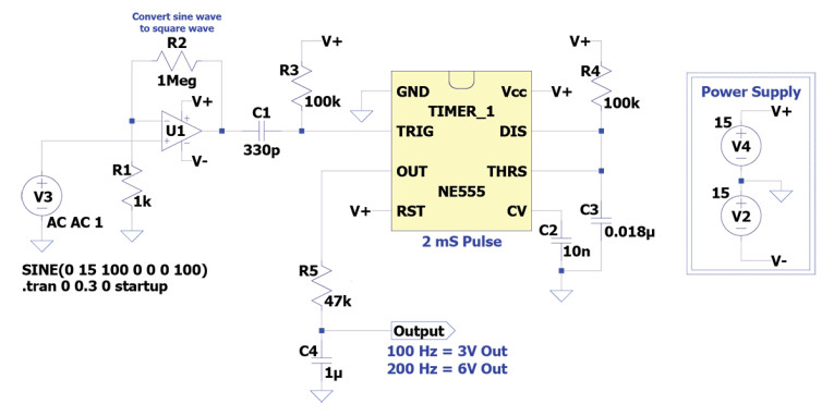
Figure 2 shows the oscilloscope display when the source is 100Hz, and Figure 3 shows the same for 200Hz. The brown traces are the 555 timer’s output pulse stream and the yellow traces are the averaged output voltage. At both frequencies it takes time for the capacitor to reach its final averaged voltage, and the output also contains ripple instead of being steady DC. The ripple can be reduced by making the capacitor larger, but that increases the averaging time! The balance between time to average and the ripple in the output is a basic problem with all frequency to voltage converters.


Period to Voltage
A better way to convert frequency to a corresponding voltage is to measure the time span between pulses, or the period of the incoming frequency. By measuring period instead of frequency the result can be known in the very first cycle. This is the approach I used for the circuits shown in Figure 4. So rather than calling them F2V and V2F, we’ll use P2V and V2P. In the glory days of DOS, in the 1980s and early 1990s, I owned a software company and was the chief programmer. So I know the value of comments that explain how computer code works, and likewise I added many comments to the circuits shown here to expand on the descriptions that follow. In order to fit them, some of the comments are in a font too small to easily read. Under Project Files is a link to the full schematic as a PDF, which can be enlarged so you can read everything clearly. The LTspice file, also available in the Supplementary Material section of the audioXpress website, has all the comments as well.

As with the F2V in Figure 1, a sine wave source is sent through a high gain op-amp to create square waves suitable for triggering a 555 timer. But unlike F2V circuits that output a rising voltage at higher frequencies, a P2V’s output voltage becomes smaller because the period between cycles is shorter. This is easily countered in the V2P’s design, but the synthesizer’s voltage controlled filter (not shown) requires a voltage that rises at higher frequencies. So a logarithmic converter is used to generate the reciprocal 1/V needed by the filter. Another log converter serves as a divider to counter the falling voltage of the V2P’s sawtooth wave’s output. Two other auxiliary circuits multiply and divide the V2P’s square wave frequency to generate simultaneous higher and lower octaves.
Circuit Details
The basic concept for reading the period of a waveform’s frequency is to start charging a capacitor when an input cycle begins, then “sample” the voltage across that capacitor when the next cycle starts. At low frequencies the capacitor’s voltage rises more than at high frequencies simply because it was allowed to charge up for a longer time period. The sampled voltage also needs to be remembered, or “held,” at a steady level until the next cycle ends. Hence the name Sample & Hold.
For clarity, this circuit uses a simple Sample & Hold rather than the more complex version shown in my previous article (audioXpress, April 2022) from the full guitar synthesizer. Working our way from left to right, then top to bottom, I’ll explain each circuit section of Figure 4 in turn.
Five separate 555 timer ICs are used in monostable mode to generate positive voltage pulses of varying duration. This popular timer IC is triggered to begin a cycle each time its input drops below one-third of the power supply voltage. As each incoming wave cycle goes from positive to negative, the first timer’s output goes high for 80 microseconds (µS) to establish the sample period for the CD4066B analog switch directly below. This timer also triggers a series of events: first a brief delay to allow the “ramping” capacitor C10 to stabilize at its final value, then another 2.5µS to discharge the cap back to zero volts to begin the next cycle. This capacitor is charged by a constant current source (CCS) rather than a resistor because charging times with a resistor aren’t perfectly linear. With a CCS the capacitor reaches exactly half the voltage when the incoming frequency rises one octave, as shown in Figure 5.

Note OR gate A1 that allows holding the ramp capacitor at zero volts in Sustain mode. Most synthesizers let you use a foot switch to emulate the Sustain pedal on a piano. In Sustain mode the current note continues to play even after the guitar’s output stops, with the Sample & Hold continuing the current note’s voltage. This circuit has been altered to function on its own, separate from the rest of the entire synthesizer, so the second OR input is grounded to disable it.
Also note that NPN transistor Q1 is reversed from its usual orientation where the emitter would be grounded with the collector connected to discharge the ramp capacitor. When a transistor is used backwards like this its gain is only 1, but it brings the emitter much closer to ground than the usual configuration, which in turn increases the linearity of the P2V conversion. However, these operations are never perfectly linear, so a teensy offset voltage is applied at op-amp U7.
The Sample & Hold circuit is based on an analog switch that opens and closes under voltage control, followed by a capacitor that holds the voltage applied when the switch was briefly closed. It’s important to use a high-quality film capacitor here because ceramic capacitors have memory effects that make them nonlinear. Ceramic caps can also “leak” some of their charge. For the same reason, an FET op-amp is used to buffer the cap’s voltage because the higher bias current of a typical bipolar op-amp would drain the capacitor over time making the note go sharp or flat in pitch.
The Sample & Hold’s output also feeds the logarithmic converter mentioned earlier that’s needed for the voltage-controlled filter elsewhere in the synthesizer. This circuit is adapted from Texas Instruments (TI) Application Note AN-30, which you can download from the link in Resources. For this LTspice emulation, common 2N3904 transistors are used to generate the logarithmic result. But the real circuit will use dual NPN transistors, where both are on a common substrate. This ensures better linearity in the conversion because ambient temperature changes will affect both transistors equally. Obviously, temperature is not a factor in a circuit emulation!
The main portion of the V2P converter is near the middle of the third schematic row, and it’s more or less a reciprocal to the P2V circuit. Like the P2V, it also charges a ramping capacitor (C14) with a CCS, which is reset when the cap reaches the incoming P2V control voltage via comparator U14. The comparator then triggers a pair of 555 timer chips that reset the cap to zero volts using another reversed transistor, Q4. A second comparator, U15, generates a square wave output, and its reference voltage can be changed either manually or via voltage control to vary the duty cycle to become a pulse wave.

Earlier I mentioned that synthesizers let you transpose notes to play in a different key, and most also let you vary the pitch for vibrato and FM effects. So only 6 microamps (µA) of current is applied to allow shifting the pitch up or down a full octave via external voltage control. If the same 12µA was used, the cap would try to exceed the 15V power supply limit at very low frequencies.
Since the voltage at the ramping capacitor is a sawtooth, we can use that for one of the V2P oscillator’s outputs. But the voltage varies directly with frequency, making higher notes softer and softer. As with ramp capacitor C5 in the P2V converter, C14 in the V2P circuit is also charged by a CCS. And as with C5, the highest voltage reached before its reset halves with each doubling of frequency. So to normalize the sawtooth wave’s output level to remain constant versus frequency, another logarithmic converter divides the sawtooth’s falling voltage by the P2V’s output voltage that is also falling. For example, 10 divided by 5 is the same as 6 divided by 3.
LTspice does not have a potentiometer component, so in the V2P converter are notes to replace resistors with pots or trimpots, for example to set the pulse width manually or to fine tune the pitch. Pulse width changes the duty cycle of the square wave output, which makes the tone thin and reedy sounding as the pulses get more narrow. This circuit shows ways to control the width both manually and via voltage control. The manual potentiometer is not connected, but could be through another 180k resistor. In case it’s not obvious, this synthesizer is still in development, though most of the modules are complete and fully functional.
The last two sections are the frequency doubling and halving, using basic logic circuits rather than separate V2P converters. Dividing a frequency by 2 is simple using a D (“Data”) flip-flop. Each rising edge at the Clock input to A2 toggles the Q and Q-bar outputs once. So it takes two cycles at the Clock input to complete one cycle at the outputs.
To double the frequency we instead use an Exclusive OR gate. In this case, each rising and each falling edge of the incoming square wave generates a new pulse at the output. Note that this output has a fixed pulse width, so the duty cycle changes with frequency becoming thinner sounding for notes at a lower pitch. This is not necessarily a bad thing for a synthesizer as it retains more body at higher notes keeping them from becoming too thin and buzzy sounding.
The audio output mixer is simple enough to be self-explanatory. I connected only one of the output waveforms, and for now used fixed resistors to set the volume levels. In the final design each signal source will have its own 10kΩ audio taper volume control, as noted in the schematic comments. The 0.1µF capacitors are needed because the V2P oscillator outputs go up from 0 volts, but audio signals must be centered around 0 volts going both positive and negative.
Author’s Note: In my previous articles I mentioned my friend Leo Taylor, who in the 1970s taught me much of what I know about audio circuits. I also need to acknowledge my current mentors, Bill Eppler and Julia Truchsess. Both are black belt-level electronics geniuses, and exceedingly nice people. The core Period to Voltage and Voltage to Period converters are Bill’s design, and Julia helped with many of my recent projects published in audioXpress. I could not have designed the Null Tester (June, 2019) without her expert guidance. Julia’s Pragmatic Designs company website contains a huge amount of fun and interesting content, including all of the musical instrument products and accessories she’s designed over the years.
Read the other articles in this Building a Guitar-Controlled Synthesizer series
Part 1 - The Sample and Hold Time Machine
Part 3 - LFO and ADSR
Part 4 - Input Section
Part 5 - VCA and VCF
Project Files
To download additional material and files, including the Sample & Hold LTspice file, visit
http://audioxpress.com/page/audioXpress-Supplementary-Material.html
Resources
LTspice,
www.analog.com/en/design-center/design-tools-and-calculators/ltspice-simulator.html
LTspice online support forum, https://groups.io/g/LTspice
Texas Instruments Application Note AN-30, Log Converters,
www.ti.com/lit/pdf/snoa641
Julia Truchsess, Pragmatic Designs, https://pragmaticdesigns.com
E. Winer, “Building a Guitar-Controlled Synthesizer: The Sample & Hold Time Machine,” audioXpress, April 2022
E. Winer, “Building a Null Tester Device,” audioXpress, June 2019,
https://audioxpress.com/article/you-can-diy-building-a-null-tester-device
This article was originally published in audioXpress, May 2022.