For those readers following the fascinating article series by Morty Tarr, this final article in the series contains an additional section with important aspects of amplifier design. In the first two parts of this article series, Tarr discussed the technical merits of cascodes and related circuits. This useful addendum covers a simple test circuit for matching FET devices, the fascinating story of the Blowtorch Line Stage design, and additional notes on inverting and non-inverting amplifier stages and integrators.
Matching Components
Many circuits have improved performance when certain semiconductor components are matched. Matching involves controlling certain parameters while measuring another parameter and selecting device pairs, triples, or quads based on these measurements. For example, we can set up a MOSFET to have a VDS of 10V and an ID of 10mA; measuring VGS under these conditions. This is how we could match the current mirror MOSFETs for the amplifiers.
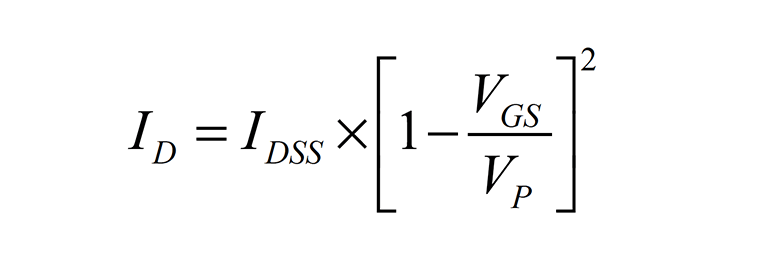
The JFET pairs should be matched for IDSS and VGS. This will minimize both distortion and offset voltage. Fortunately, matching for VGS at the operating point (ID) is sufficient as VGS and IDSS are related for JFETs:
Matching Fixtures for MOSFETs and BJTs
In Figure 20, Q1 and Q2 are the devices to test. It is okay to just use one test socket at a time. Q3 is for the AD711, which had an output phase shift when starting up. C1–C4 prevent oscillations (this circuit has lots of feedback), reduce noise, and stabilize the measurement.
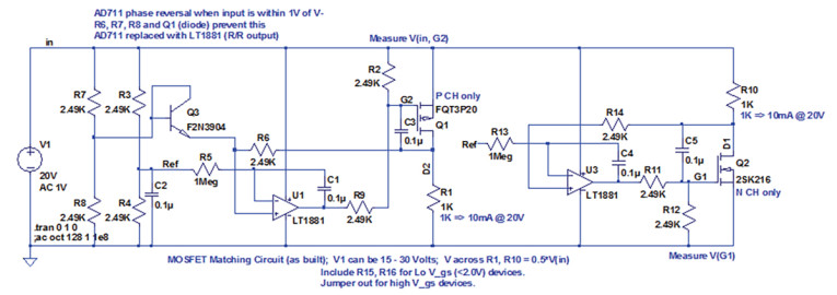
I use this fixture with a single 20V supply, which means there will be 10V across each MOSFET. With R1 and R10 = 1kΩ, there is 10mA ID current.
I measure VGS for each MOSFET and tape the devices to a sheet of paper where I can write down the measured parameter.
Note that as the device is powered up, the die temperature is changing and the measurement will be changing as well. I wait 10 seconds after power up and take the measurement. The value is still changing at that point, but it has worked for me so far.
If we standardize on a 20V power supply, current through the device under test (DUT) can be changed by changing resistors R1 and R10. The voltage across the DUT is set by the divider R3 and R4. The ratio can be changed to change the voltage across the DUT. If you do this, you will need a separate divider for the N-Channel and P-Channel portions of the test jig. For more information, read Nelson Pass’ article on device matching (see Resources).
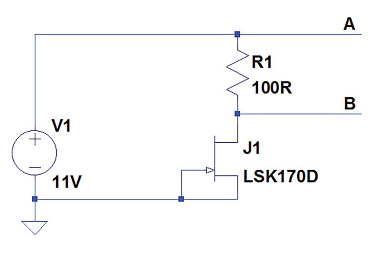
There is a simple way to match JFETs for IDSS. Referring to Figure 21, we measure across R1 (A to B), and multiply the voltage by 10. This number is IDSS in milliamps. We can adjust V1 to get 10V across the JFET (or whatever voltage we need).
I have found that running JFETs at about 10V VDS puts them at a good operating point for the cascode and the current mirror amplifiers.
In general, a 3-1/2 or 4-1/2 digit digital voltmeter (DVM) will work to make these measurements. Either way, you will see the measurement drift as the die heats up.
We are looking to match devices, so any DVM can be used (calibration is not important), so long as its input capacitance does not make the circuit oscillate. Our goal is to use two (or three or four) devices that measure the same, or close to the same.
I set the supply voltage so the voltage across the JFET is 10V. With a 10mA IDSS, the voltage at point A will be 11V.
A Case History: the Blowtorch Line Stage
To provide a little background information, my research for the line stage designs discussed in Part 2 of this article started about 10 years ago. I discovered Dimitri Danyuk’s compilation of John Curl’s publications and blog posts, “Condemnation without Examination is Prejudice” online (see Resources).
After some reading, I became determined to hear a Blowtorch line stage. Since John Curl was no longer building them (and he wanted in excess of $10,000 to purchase one), my option was to make one myself. There was plenty of information in the document, and much more in the Blowtorch threads on the diyAudio website.
At some point, I had enough information to re-create the design. I also decided I wanted to meet John Curl. We actually met at CES about a year later. I was able to visit him in California and he gifted me several pairs of Toshiba 2SK389/2SJ109, which were matched to each other. I use those devices to compare the results obtained with the Linear Systems and other devices to insure that performance is not degraded.
Six years ago, I had PCBs fabricated and built my version of the Blowtorch line stage. I used IRF510 and IRF9510 MOSFETs as John did, and I was disappointed to get distortion in the -50dB range even at output levels of 2V to 4VPP, indicating a problem. A quick call to John resulted in the additional information that IRF P-Channel devices were not linear enough. John had used Fairchild MOSFETs, and I needed to purchase a curve tracer.
Fairchild (now OnSemi) no longer made IRF510s and IRF9510s. But the company had the FQP3N30 and the FQP3P20, which have similar specifications. That made a significant difference, as these devices were much more linear. Now I had distortion better than -80dB.
I thought I could improve the design further (my goal was distortion products better than -90dB, which is 0.0032%). This involved converting the resistor current sources to active current sources and experimenting with different MOSFETs. Using active current sources, I was able to reduce the current in the output stage to 10mA (John’s design has about 40mA in the output stage). I suspect the reason for the higher current is to minimize the change in VGS with signal level,
By trying different combinations of FQP3N30 and FQP3P20 devices, I could get distortion products as good as -88dB, but I was unable to determine which characteristics resulted in this performance. Exicon lateral MOSFETs allowed me to get to about -93dB distortion products (0.0022%), but it seemed excessive to use 200W lateral MOSFETs as devices dissipating only 250mW. This is the best distortion performance I have been able to achieve so far. I have also achieved -93dB with Microchip (formerly Supertex) VP2450 and VN2450 MOSFETs, and Diodes, Inc. (formerly Zetex) ZVP4424A and ZVN4424A MOSFETs.
My measurement system is not state of the art, consisting of a HP339A analog THD+N analyzer, which has the meter output connected to an HP 3580A spectrum analyzer. The spectrum analyzer shows the distortion products present, and I look for distortion to be limited to second and third harmonics until the signal gets close to clipping. Using an Audio Precision would likely yield better results, as the fundamental could be fully removed and the noise could (optionally) be discounted. Also, it would make the measurement sequences much faster to acquire and record.
Starting with the Blowtorch
Figure 22 shows John Curl’s circuit for the Blowtorch line stage. (It originally appeared in the diyAudio Blowtorch thread and on page 88 of the “Condemnation without Examination is Prejudice” article.)
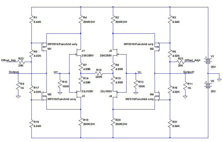
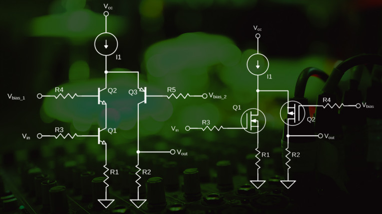
John Curl invented this topology, and it is brilliant! JFETs J1 and J3 create a constant current source that is also the input buffer. Similarly, JFETs J2 and J4 create a constant current input buffer. The difference between in+ and in- is impressed across R10, the gain resistor.
The biasing resistors, with ±25V supplies, puts the sources of the MOSFETs at about ±15V, which sets the current in the 200Ω resistors to about 50mA. This equates to 10mA for the JFETs and 40mA for the MOSFETs. Note that the input resistors, R12 and R13, can be 100kΩ or higher. An unused input should be shorted to ground (for lowest noise and offset).
My circuit design for the Blowtorch line stage substitutes current sources for the 200Ω resistors. I found I could get better distortion with lower current, so my current sources are 20mA (10mA each for the JFETs and MOSFETs).
This design is the origin of the circuits presented in Part 2 of this article series (audioXpress, November 2021). As it is very expensive to get sufficient quantities of JFETs to match the IDSS of the N-Channel and P-Channel JFETs to each other today, I modified the design so that matching P-Channel to N-Channel devices is less critical. My design has the additional benefit of creating twice the current in the gain resistors, as the current is created between the N-Channel JFETs and also between the P-Channel JFETs vs. once in John Curl’s design.
Note that if you can tolerate some additional noise, MOSFETs can be used in place of the JFET input devices that are shown in Figure 17 and Figure 19 from
Part 2 of the article series. The MOSFET N-Channel and P-Channel pairs should be matched for
VGS at 10mA, but the N-Channel and P-Channel devices do not have to match each other. Distortion performance is about equal to the JFET input stage (Photo 1).
Inverting vs. Non-Inverting Amplifier Stages
Referring to the two line stage designs in Part 2 of the article series, the Cascode Line Stage is inverting as the signal connected to in+ produces out- directly. This means that if we use the amplifier as a single-ended stage (in and out), our output will come from the side of the amplifier whose input is grounded. While this may seem like a bad idea, it is actually good in the same way a cascode is good. There is no change in the gate-drain capacitance of the JFETs whose gates are grounded, which results in marginally better performance. The difference is on the order of 1dB to 2dB better distortion, which is not necessarily audible, but is measurable. The Current Mirror Line stage is non-inverting. The advantage here is that we can choose to have gain, and/or use simpler inverting integrators for DC servos.
There are several things I’d like to point out about building these circuits, should you decide to do so.
LED Strings
I have built a number of these circuits. While assembly techniques usually call for assembling the lowest profile devices first, and moving to higher profile devices in order of their height above the PCB, I have found that this may not be the best way to assemble this design.
I install the LED bias strings first. With just the LEDs and their biasing resistors installed, I apply power to the PCB. All the LEDs should illuminate! If some do not, there may be an LED inserted backward or a defective device. I have found defective devices to be very rare.
In order to find a backward LED, use a clip lead to connect a resistor to ground (the value is not critical, I use 4.99K). Starting at the LED closest to the power supply, touch the other lead of the resistor to each LED in turn until you find one that does not illuminate. That will be the backward device. Note that the LED strings should be bypassed with capacitors. This is not shown in the schematics detailed in Part 2 of the article. I used 1µF film caps for this.
If at any time during debug and bring-up there is an LED that does not illuminate, this indicates a problem. Once the amplifier is fully assembled, it is harder to find a backward LED.
Power Dissipation
When we design circuits without global feedback, it is important to be careful with regard to device power dissipation. It is best to limit the dissipation to one-third, or at most, one-half of the device rating. This helps each device maintain a constant temperature and minimizes drift from changing device temperature. We do not want device temperature to change once it is warmed up, and especially to not change with input signal.
The reason power dissipation is more important without global feedback is that many devices change value (even slightly) with changing temperature. In a feedback amplifier, the feedback will correct for minor changes with minimal impact on performance. Without feedback, the value is not “corrected.” If we think of a simple single stage amplifier, imagine the collector resistor changing value with signal level due to power dissipation changes. This change can even follow the signal. As the resistor value changes, the gain changes, causing distortion. Without feedback, it is prudent to insure that device temperatures stabilize and do not change with input signal.
Power Supplies
In the article, we have not talked about power supplies. Amplifier performance can be affected by the power supplies to which it is connected.
The amplifiers presented in the article do not have a great Power Supply Rejection Ratio (PSRR) as many op-amps do. So the quality of the power supply is a significant concern with regard to amplifier performance.
Our goal for a power supply is to convert the AC line voltage to a DC voltage emulating an ideal battery; that is a DC voltage with virtually no ripple and no noise. Also, we want the power supply to be such that each amplifier is isolated from all the other amplifiers in the system.
There is not room here for a treatise on power supplies for audio, but a few recommendations are in order.
Be mindful of the noise in the power supply output voltage (Zener diodes are noisy). If the output impedance of the power supply is significant, add a capacitance multiplier stage for each individual amplifier to isolate the amplifiers from each other.
Use heatsinks for power transistors, if required.
Use good quality capacitors to decouple the power supply at the PCB, and at points where the current draw can change with the input signal.
A capacitance multiplier can be effective for reducing power supply noise and preventing channel to channel crosstalk through the power supply. A capacitance multiplier can be made with BJTs or MOSFETs. Capacitance multipliers provide isolation when each circuit section has its own capacitance multiplier. Figure 23 shows an example of a BJT capacitance multiplier.
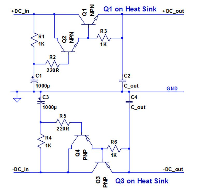
A BJT-based capacitance multiplier has a voltage drop of about 1.5V. Q1 and Q3 are devices that handle the full supply current of the amplifier, and may need to be attached to heatsinks (depending on the current draw). Q2 and Q4 are small signal transistors, included to insure there is sufficient current gain.
R1 and C1 filter the input DC signal. The filtered signal is applied to the base of Q2 and then to the base of Q1 via Q2.
R2 is present to ensure that the emitter followers do not oscillate. R2 should be located close to Q2. Figure 24 shows an example of an MOS capacitance multiplier.
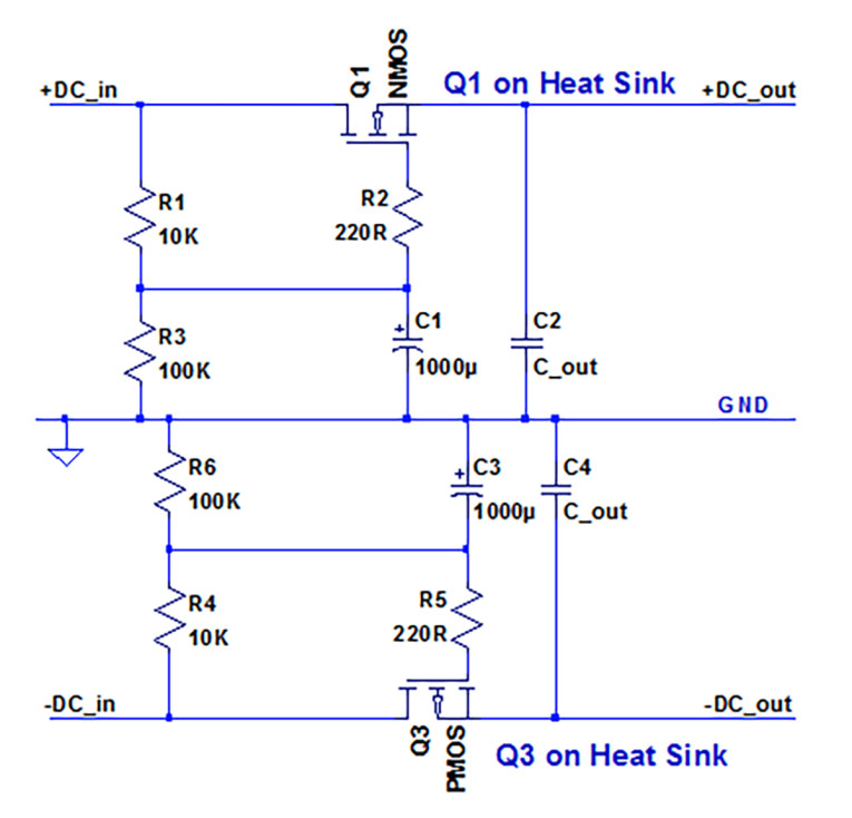
In the MOSFET version, we do not need Q2 and Q4 as the impedance at the MOSFET gate is very high. R2 and R5 should be located close to the gates of Q1 and Q3 to prevent oscillations. Since MOSFETs have a 3V to 5V differential from gate to source, we include voltage dividers R1/R3 and R4/R6 so the devices do not saturate. The voltage divider technique could be used with the BJT capacitance multipliers as well.
There are experts who advise that the output capacitors should not be electrolytic capacitors, but should be only high-quality film capacitors. If you do this, the decoupling capacitors in the amplifier following the capacitance multiplier should be equally high-quality film capacitors.
Inverting and Non-Inverting Integrators
Integrators are important tools for finding average values. We use integrators as low-pass filters for DC servos in amplifiers. The basic idea is that the input of a servo is connected to the amplifier output. The output of the servo then represents the average or DC part of an amplifier output. By feeding this back to a suitable point in the amplifier, the servo can null the amplifier DC output. Amplifiers can be inverting or non-inverting so sometimes you need an inverting servo, at other times a non-inverting servo. Both types are discussed next. An inverting integrator is the simplest to make.
For the circuit shown in Figure 25, the time constant is R1 × C1 and a –3dB point of F = 1/(2 × π × R1 × C1). For R1 = 1 MΩ and C1 = 1µF, we have a time constant of 1 second and a -3dB point of 0.167Hz.
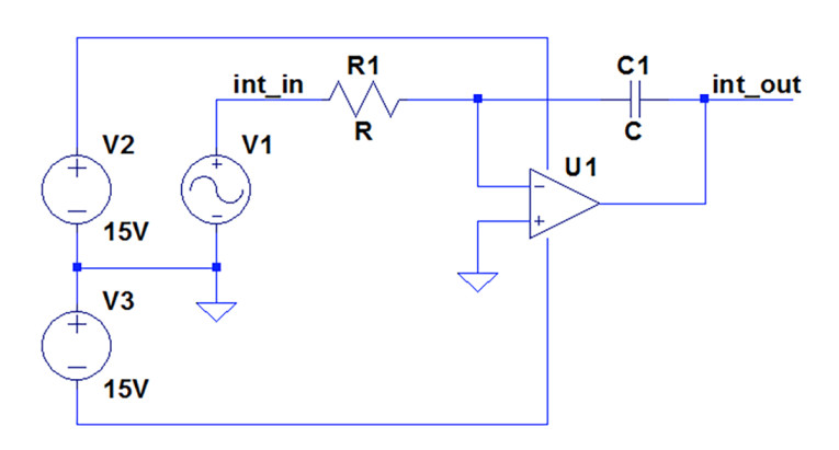
Note that the circuit shown in Figure 25 compares the input voltage to GND, and the op-amp output moves to keep the node intin at GND. In this inverting integrator, intout moves in the opposite direction of intin.
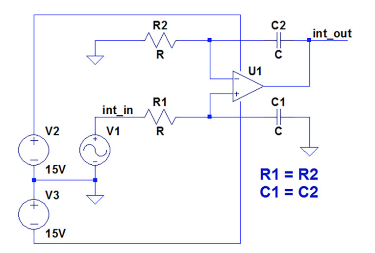
If our circuit is inverting, then we might need a non-inverting integrator. For a non-inverting integrator (Figure 26), the time constants R1 × C1 and R2 × C2 must match. The time constant is equal to R1 × C1 as in the inverting case. The -3dB point is F = 1/(2 × π × R1 × C1), also the same as the inverting case. For the non-inverting integrator, intout moves in the same direction as intin.
In Conclusion
This three-part series is a brief description of some of the important aspects of amplifier design. It is by no means a comprehensive review of everything we need to know about amplifier design. VC
Resources
Blowtorch threads, diyAudio website:
Part 1: www.diyaudio.com/forums/solid-state/71189-john-curls-blowtorch-preamplifier.html
Part 2: www.diyaudio.com/forums/the-lounge/146693-john-curls-blowtorch-preamplifier-ii.html
Part 3: www.diyaudio.com/forums/the-lounge/318975-john-curls-blowtorch-preamplifier-iii.html
J. Curl, “Condemnation without Examination is Prejudice,” May 2006,
http://jockohomo.net/data/johncurl-v.0.1.pdf
N. Pass, “Matching Devices,” Pass Laboratories, Inc.,
www.passdiy.com/project/articles/matching-devices
Read Part 1 of this article here.
Read Part 2 of this article here.
 About the Author
Morty Tarr has more than 30 years’ experience in Electrical Engineering. Morty graduated from Cornell University in 1972 with a Bachelor of Arts in Physics, and a minor in Electrical Engineering. He continued his studies at Tufts University in Electrical Engineering.
Morty began his career at recording studios in NYC and Boston. Then he started to be interested in the design of electronic equipment and made the transition from audio to electronic design. He has extensive experience in the fields of video, audio, test and measurement, networking, and wireless (primarily Wi-Fi and Bluetooth). More recently, from 2006 to 2015, Morty led a team at Bose responsible for advanced development for a $2 billion business. He set the direction for the group and for technology strategy spanning wireless, digital, analog, and system architecture across multiple product lines. Prior to Bose, he worked for LTX developing GHz test systems, at Octave Communications developing conference call bridges, and at Avid Technology. Prior to Avid, at Data Translation, he created the first 24-bit resolution A/D for a PC for Chromatography applications, and then led the team that developed the first Media 100 video editing system. Morty currently has 20 patents and has spent most of his professional career developing first-in-class products. Innovative ideas and new concepts come naturally to him.
This article was originally published in audioXpress, December 2021