
Cascodes and Folded Cascodes
As designers, we have many devices from which to choose. Some devices are ideally suited to certain tasks. Other tasks require performance that is difficult to achieve. While many excellent devices exist today, ideal devices do not exist, except maybe in Spice simulations.
Cascodes, folded cascodes, and current mirrors are circuit topologies that are used to provide specific functions for an amplifier design. These topologies improve the performance of the devices, but also add complications to the design.
Why Would We Need a Cascode?
Figure 1 shows a basic NPN voltage gain stage. Transistor Q1 is operating in common emitter mode, where the base terminal is the input, the emitter is connected to ground, and the output is taken from the collector. The gain is equal to R2/R1 (inverting) where R1 includes the emitter resistance of Q1. Since the emitter resistance of Q1 varies with current, it is important that R1 be larger than the ~26Ω/mA resistance of the emitter.
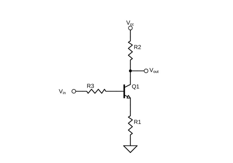
There are several factors that limit the bandwidth and linearity of the amplifier in Figure 1. In a common emitter gain stage, the capacitance between the base and the collector terminals of the transistor feeds the output signal (the collector voltage) back to the base (the input terminal). As the frequency increases, the impedance of the base-collector capacitance decreases. This contributes to the frequency response roll-off at high frequencies, especially since we like high input impedance for our gain stages. The collector-base junction capacitance varies with collector-base voltage. Higher voltages correspond to lower capacitance. This is the Miller Effect or Miller Capacitance.
Transistors also exhibit a phenomenon named after James Early, who discovered it. In a bipolar transistor, the width of the base region is modulated by the base-collector voltage. The width of the base affects the gain (β, or HFE) of the device. Smaller base widths correspond to higher gain. As the collector voltage of a transistor increases, the base width becomes smaller and the gain increases. This is illustrated in Figure 2.

The Early Voltage (VAF in Spice) is an extrapolation of the constant VBE curves to a point on the horizontal axis. Larger (more negative) values indicate a smaller Early Effect.
If the effective gain of the transistor can change with signal level, the stage will create distortion. A typical goal of 0.01% distortion is 1 part in 10,000. This can be easily exceeded by the Miller Effect and Early Effect. These effects can be mitigated via feedback, cascodes, or a combination of the two.
Cascodes are not new. Cascodes were and are used in tube circuits, particularly in high-frequency designs. In this article, we’ll focus on solid-state devices.
BJT Cascodes
Let’s start with a basic bipolar junction transistor (BJT) cascode. Figure 3 shows a basic cascode circuit. Q1 is the input transistor and Q2 is the cascode transistor. The voltage gain is given by R2/R1 and is inverting just like a single transistor gain stage.
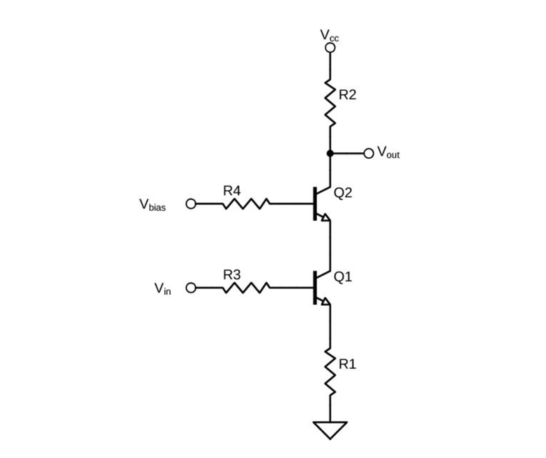
Gain transistor Q1 is operating in common emitter mode, with the base as its input. This is where our signal is applied. Cascode transistor Q2 is operating in common base mode (the base is connected to a DC bias voltage), its input is the emitter terminal.
Here’s how it works. As voltage Vin increases, the current in Q1 increases. Since the only place this current can go is through Q2, the current in Q2 increases. VBE of both Q1 and Q2 also increases due to the higher current, so the bias at the collector of Q1 changes, but only slightly. The current in Q2 is then impressed on R2, rising current driving voltage Vout toward ground. As Vin decreases, the voltage at Vout increases in a similar but opposite manner. This is pretty much the same as if we didn’t include Q2 and R4.
Adding Q2 provides several advantages. With Q2 in place, the collector of Q1 is held at an almost constant voltage. This minimizes the effect of the base-collector capacitance (the Miller Effect) thereby increasing the bandwidth of the gain stage. Holding Q1C at a constant voltage also minimizes Q1’s Early Effect.
As an example, if we bias the base of Q1 in Figure 3 at a constant DC voltage, and increase the voltage at the base of Q2, we are increasing the collector voltage of Q1. As we do this, the gain of Q1 will increase with a corresponding effect on the collector current of Q1, even though we did not change the DC bias voltage Vin.
This is not an effect we want. If the gain of the stage changes with signal voltage, distortions will result. We’d like the gain of the stage to be independent of the signal, at least until we get close to clipping.
The cascode transistor Q2 prevents the collector of Q1 from moving more than a few tens of millivolts, thereby minimizing the Early Effect as well and the feedback capacitance. Note that there is no requirement for Q1 and Q2 to be the same type of device. Q1 can be a low voltage high β device, and Q2 can be a high voltage, lower β device. The β of Q2 determines only how much base current it draws through R4. With a cascode, R4 is almost always required to reduce sensitivity to oscillation. Usually 100Ω to 1kΩ is sufficient.
Devices designed for higher voltage have thicker bases, therefore, they have lower β. They also have a higher voltage at which the Early Effect becomes significant. Unfortunately, the Early Effect is not mentioned in device data sheets. Nor is the Early voltage, which is extrapolated from the slope of the constant VBE curves of the device. For an amplifier stage, a higher Early Voltage is desirable, as this will minimize the gain changes with signal level.
We set up the cascode so the gain transistor, Q1, has a nearly ideal collector-emitter voltage. This is generally in the 5V to 10V range. To do this, we set the DC voltage Vbias at about 10V higher than the DC component of Vin. The base-emitter junction of Q2 will drop about 650mV, so we will have 10V – 0.65V = 9.35V across Q1. A higher voltage across Q1 makes it more linear, but then we can run into power dissipation issues if the current is significant. Q2 can be a high voltage transistor (e.g., the KSC2690 or KSC3503). The larger packages also allow significantly more voltage across the device without running into power dissipation limits.
Please don’t try to use a cascode without base resistors. The high gain and high-frequency response are very likely to cause oscillation. Also, you should not put a decoupling capacitor at the base of Q2; that is about the same as omitting R4. In practice, I test to make R4 as small as I can without oscillation and then use double that value. Generally, R4 = 220Ω is a good starting point.
Note that in the cascode configuration, Q2 provides a current gain of just under 1.00. In other words, the current at R2 is the same as the current at R1 (less the base currents of Q1 and Q2).
Although we have illustrated these effects with NPN bipolar transistors, they apply to PNP transistors as well. MOSFETs also have many similarities. In a MOSFET, the drain-gate capacitance is the feedback capacitance, Crss. The equivalent of the Early Effect is the channel length modulation. So we can’t really get away from these issues with today’s technology. A cascode stage with N-Channel MOSFETs is shown in Figure 4.

MOSFET Cascodes
A MOSFET cascode has much lower bias current as the gates of the field-effect transistors (FETs) draw orders of magnitude less current than the bases of bipolar transistors. Also, the gate-source voltage of most MOSFETs is in the 4V to 5V range, where the base-emitter voltage of a BJT is in the 600mV to 800mV range. This means that the difference between Vbias and Vin has to be 4V to 5V higher than in the BJT case.
Although it may not be obvious in the case of MOSFETs, “interesting” things happen if we let the drain voltage approach the gate voltage. These effects include significant changes in node capacitances and stored charge as VDG approaches zero volts. These effects can be mitigated in switching circuits, but not so much in linear designs. So keep the drain voltage higher than the gate voltage. I find a 5V difference to be a good minimum, with 10V ideal, but often hard to achieve.
Folded Cascodes
A cascode increases the bandwidth of a gain stage and its inherent linearity. It would be good to be able to have these advantages, and also reverse the polarity to bring the signal level back down to ground, or near ground. A folded cascode can do this. Figure 5 shows a BJT folded cascode.

In a folded cascode, the cascode transistor is the opposite polarity of the gain transistor. In this example, Q1 is the input (an NPN transistor) and Q2 is the folded cascode (a PNP transistor). Current source I1 provides the operating current for Q1 and Q2. The current in Q2 is the current supplied by I1 less the current consumed by Q1. As Vin rises, the current in Q1 increases, so the current in Q2 decreases and Vout also decreases. The stage is inverting, just as the basic cascode.
Note that the voltage at the emitter of Q2 will change with the current in Q2. As the current in Q2 increases, the emitter voltage of Q2 will also increase as VBE of Q2 increases, so if we’re using a resistor for the current source, there will be small changes in the total current. For precision, I recommend a current source rather than a resistor for I1. The change in current in Q2 is equal to the change in current in Q1, so the gain of the circuit is still R2/R1 (inverting).
The emitter of Q2 is again kept at a reasonably constant voltage, so the feedback capacitance of Q1 has minimal impact on the frequency response. Here Q2 must be a different device, although it could be what we call a complementary device. In reality, NPN and PNP transistors (and N-MOS and P-MOS FETs) are not truly complementary, but that is a topic for another article.
In a basic cascode, the DC current in Q1 and Q2 is the same; in a folded cascode the DC current in Q1 and Q2 can be different. However, the AC current in Q1 and Q2 will be the same, as the current changes in Q1 are the same magnitude but opposite polarity of the current changes in Q2. Cascodes do not provide current gain. We can make a folded cascode with MOSFETs as well.
Figure 6 shows a folded cascode that is very similar to the BJT example. VGS of the MOSFETs is higher than VBE of the transistors, so we have to accommodate that in the biasing of the devices. Q1 is an N-Channel MOSFET and Q2 is a P-Channel MOSFET. We do not want either Q1 or Q2 to saturate as that would be really bad for linearity.

Figure 6: This is a schematic for a folded cascode that is very similar to the BJT example.
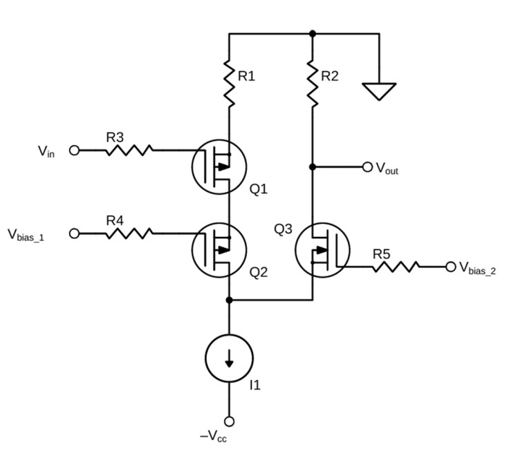
We can combine a basic cascode and a folded cascode as shown in Figure 7. We would do something like this if we were making an amplifier where we needed a large output swing, but we wanted to use a lower voltage device for input transistor Q1. Q2 allows Q1 to function at a lower (and almost constant) collector voltage while the output at Q3 can be a much larger voltage. Q3 would ideally be a device with a high Early Voltage to minimize the effects of β changes. An example of these requirements is the input stage of an audio power amplifier.
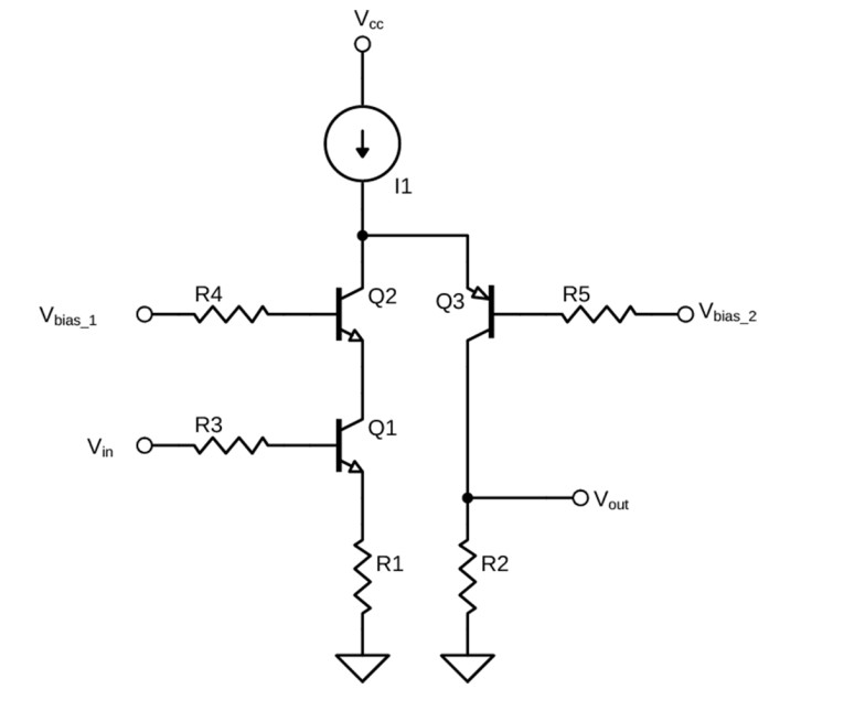
The input transistor is Q1, cascoded by Q2 whose emitter sets the collector voltage for Q1. The emitter voltage of Q3 sets the collector voltage of Q2, and again the voltage at Q3’s emitter will change with the current conducted by Q3.
P-Channel Cascodes
Cascodes are not limited to N-type devices; a P-Channel cascode is also possible. For the schematic in Figure 8, input transistor Q1 is a PMOS device. It is cascoded by Q2, also a PMOS device. The cascode is then folded by Q3, an NMOS device.
Note that in each of these examples, we could have a BJT or MOSFET cascode with a JFET input, or a BJT cascode with a MOSFET input, or any combination that makes sense for the design requirements. We are not constrained to use the same or even similar devices (as some silicon designers are constrained by integrated circuit process parameters). For example, in Figure 8, Q2 could be a PNP transistor and Q3 could be an NPN transistor.
In Part 2 of this 3-part article series, we will discuss current mirrors and line stages built with cascodes, folded cascodes, and current mirrors. aX
Author’s Note: I would like to thank John Curl for generously sharing his time, knowledge and insight.
Read Part 2 of this article here.
Read Part 3 of this article here.
 About the Author
Morty Tarr has more than 30 years’ experience in Electrical Engineering. Morty graduated from Cornell University in 1972 with a Bachelor of Arts in Physics, and a minor in Electrical Engineering. He continued his studies at Tufts University in Electrical Engineering.
Morty began his career at recording studios in NYC and Boston. Then he started to be interested in the design of electronic equipment and made the transition from audio to electronic design. He has extensive experience in the fields of video, audio, test and measurement, networking, and wireless (primarily Wi-Fi and Bluetooth). More recently, from 2006 to 2015, Morty led a team at Bose responsible for advanced development for a $2 billion business. He set the direction for the group and for technology strategy spanning wireless, digital, analog, and system architecture across multiple product lines. Prior to Bose, he worked for LTX developing GHz test systems, at Octave Communications developing conference call bridges, and at Avid Technology. Prior to Avid, at Data Translation, he created the first 24-bit resolution A/D for a PC for Chromatography applications, and then led the team that developed the first Media 100 video editing system. Morty currently has 20 patents and has spent most of his professional career developing first-in-class products. Innovative ideas and new concepts come naturally to him.
This article was originally published in audioXpress, October 2021