Current Mirrors and Line Stages
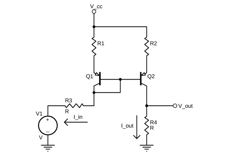
In addition to cascodes and folded cascodes, another method to improve the performance of a basic amplifier is to use a current mirror. A basic current mirror is shown in Figure 9. The inputs and outputs of a current mirror are currents, not voltages. In Figure 9, an input current is applied to PNP transistor Q1.
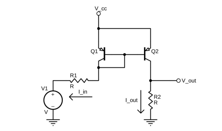
Figure 9: In this basic current mirror, the inputs and outputs are currents, not voltages. Here an input current is applied to PNP transistor Q1.
Q1 functions as a diode, so the current Iin is applied across the base-emitter junction of Q1. It is assumed that Q2 is matched to Q1, so Q2 has the same base emitter voltage and therefore the same collector current (however, this is not exactly true, we’ll get to that later). For current mirrors, the input is a current sink, and the output is a current source.
Current Mirrors
Current mirrors are used extensively in op-amp design, as matched transistors are easy to create and the supply voltages are limited. This is not the case with discrete designs.
So far, current mirrors seem very simple, where can it go wrong? In discrete designs, the matching of the transistors may not be ideal, and the temperature tracking will not be ideal. To minimize the impact of imperfectly matched transistors, we add emitter resistors. These resistors also serve to reduce the noise generated by the current mirror. Remember, the devices do not know they are a current mirror; they have a high impedance collector load (a current) and a small emitter resistance (approximately 26Ω at 1mA with no additional resistor). This is the formula for a very high gain.
Figure 10 shows a current mirror with emitter resistors R1 and R2 added. We also add base resistors to suppress the tendency to oscillate as shown in Figure 11. Figure 11 shows a current mirror adapted to discrete design. The input to the current mirror is a current, which can be applied using a voltage source and a resistor, or an active device such as a BJT (Q3), JFET (J1), or MOSFET (not shown).
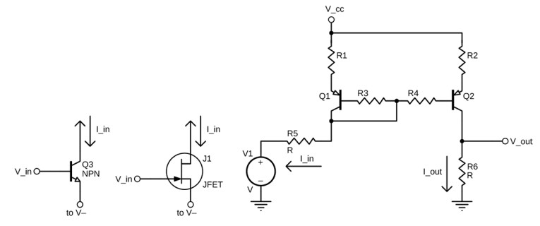
Note that an active device of the proper polarity can be the input to any current mirror. In the schematics that follow, only a voltage source and resistor will be shown, but in all cases, an active device could be used instead.
The value of the emitter resistors should be as high as you can stand it. If it is a current mirror operating at 1mA, a 1KΩ resistor will drop about 1V and dissipate 1mW. If the current mirror is operating at 10mA, a 1KΩ resistor will drop about 10V, and that’s going to be too much. So something between 100Ω and 500Ω might be appropriate. Just remember, as the resistor gets smaller, the ability to minimize any mismatch decreases and the noise gain increases. As in most designs, there are many trade-offs!
The circuit in Figure 11 will not make a very good current mirror for audio. A good current mirror should have a very high output impedance since the output is a current. The output impedance of the circuit in Figure 11 is in the tens of kilohms. We can increase this with, guess what, a cascode.
Also, we want Q1 and Q2 to match, but their operating conditions do not match. Q1 has a collector-base voltage 0V and Q2 has a much greater collector-base voltage. We can add a cascode to just the output and make a Wilson Current Mirror (there are both three and four transistor versions of the Wilson Current Mirror), or we can add a cascode on both sides as shown in Figure 12 and make a cascode current mirror.
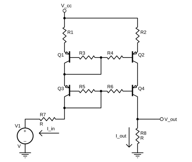
The cascode raises the output impedance by about two orders of magnitude, greatly improving performance. It also enables Q1 and Q2 to have very similar operating conditions, which also improves performance.
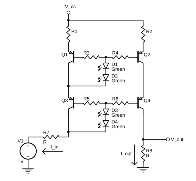
Note that the current gain is less than 1.00 by a factor of four base currents (4% if Beta = 100). This would not be problem if Beta was constant (but Beta changes with collector current). Also, Q1 and Q3 are operating at a collector-base voltage of 0V, which is not a good operating point for a transistor in a linear circuit. We can add LEDs to the design to increase the collector-base voltage of Q1 and Q3.
Since the transistors draw only microamperes of base current, LEDs are a good (low noise) choice for increasing the collector-base voltage. Green LEDs drop about 1.7V each in this configuration (1.9V to 2.1V with a 5mA current).
Bipolar junction transistor (BJT) current mirrors can be made with NPN or PNP transistors. Figure 13 shows a PNP current mirror that will reflect against the positive rail. An NPN current mirror will reflect against the negative rail. BJT current mirrors suffer from Beta changing with collector current. While the change is small, it creates second harmonic (2H) distortion. A metal-oxide semiconductor (MOS) current mirror can mitigate this problem.
There are other forms of current mirrors, but due to limited space we cannot discuss them here.
Figure 14 shows the current mirror of Figure 13 with the BJTs replaced by metal-oxide semiconductor field-effect transistors (MOSFETs). The MOSFETs contribute much lower levels of 2H distortion compared to BJTs.
When I use current mirrors in audio circuits, the best matched devices become Q1 and Q2. The match requirements for Q3 and Q4 do not have to be as good. It is better to use high voltage devices, especially for Q3 and Q4 due to channel modulation effects.
There are significant differences between current mirrors and a folded cascode. Current mirrors are non-inverting and current mirrors can have gain. A current mirror with gain is shown in Figure 15.
Figure 15 shows the same current mirror as
Figure 14, but with Q5, Q6, and R3 added. Q5 is matched to Q1 and Q2, Q6 is matched to Q3 and Q4. This configuration has double the output current of the circuit shown in Figure 14. The concept can be extended to include additional output mirrors so long as reasonable matching can be maintained.
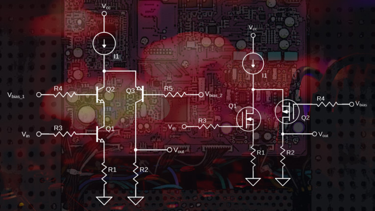
Folded Cascode Line Stage
An amplifier can be built using cascodes, folded cascodes, and/or current mirrors. An example of a folded cascode line stage is shown in Figure 16.
Note that the current sources are biased from a string of forward-biased LEDs. I chose green LEDs, which are about 2V each. LEDs provide a low noise, low impedance bias point for the current sources. Zener diodes above 5.6V are actually avalanche diodes and contribute significant noise, which is hard to filter out.
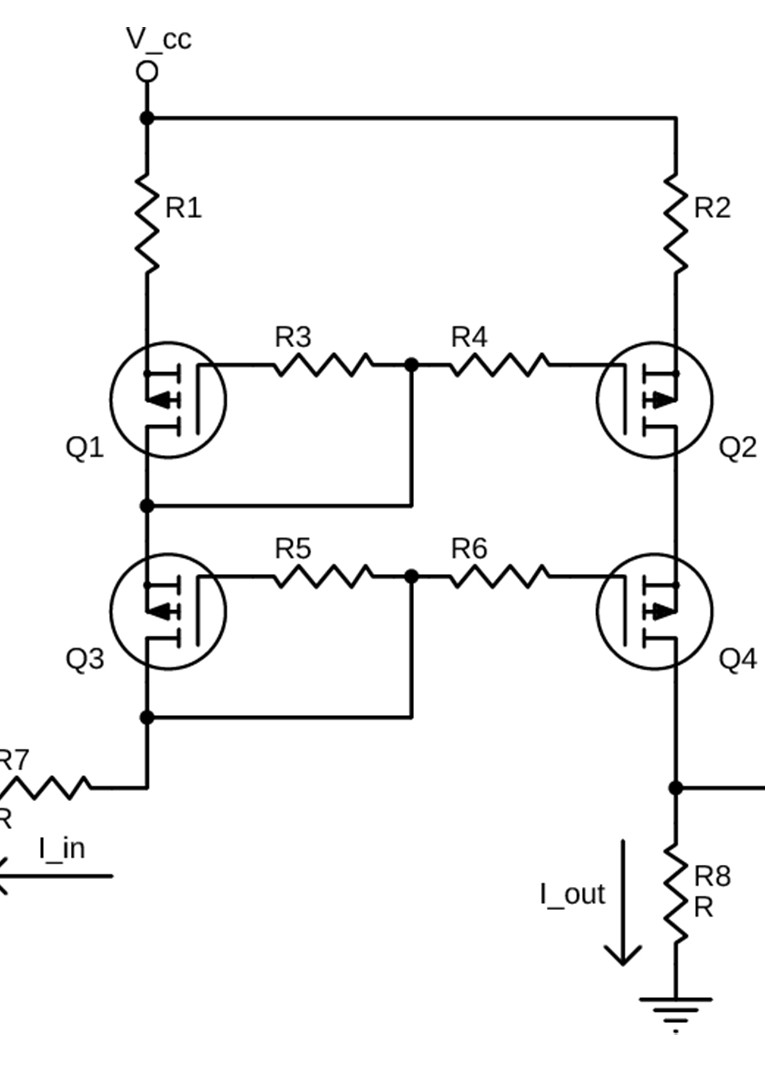
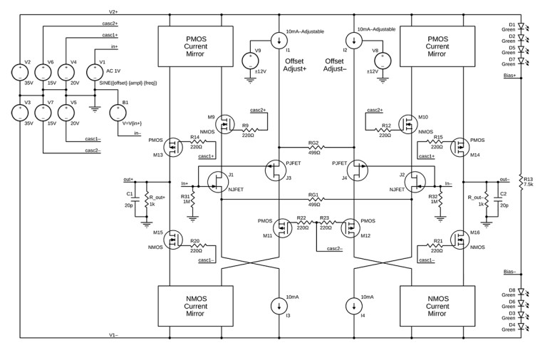
Figure 16 shows the “block diagram” of a line stage using cascodes and folded cascodes. The block diagram is easier to follow than the actual schematic (Figure 17).
Note: In the original printed article of “Cascodes, Folded Cascodes, and Current Mirrors (Part 2): Current Mirrors and Line Stages (audioXpress, November 2021), there was a connection missing in Figure 17, which is now included in this version - highlighted in red.
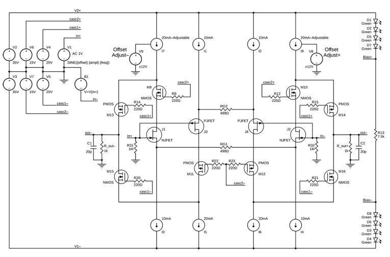
A note about terminology: The gate of a device will be designated with a G suffix, the source an S suffix, and the drain a D suffix. The gate of J1 will be J1G, the source, J1S, and the drain J1D.
The input stage includes J1, J2, J3, J4, the input JFETs. J1 and J2 are biased by current sources I1 and I2. J3 and J4 are biased by I3 and I4. The current sources are set to 10mA, which is good operating current for the JFETs. The drains of the JFETs are cascoded by M9, M10, M11, and M12. The cascodes keep the JFET drain voltage constant and also limit the dissipation in the JFETs.
Since any errors in this circuit show up as distortion, we want to treat the JFETs as “nicely” as possible. J1 and J2 are Linear Systems LSK389Ds, dual, high transconductance N-Channel JFETs. J3 and J4 are LSJ74Ds. Since the JFETs are operated at 10mA, we want I(DSS) of the JFETs to be at least 12mA to account for signal currents. Since Linear Systems does not offer a dual, high-transconductance P-Channel JFET, the LSJ74s should be matched for I(DSS).
JFETs J1–J4 form a four-quadrant voltage to current converter. J1 and J2 are matched N-Channel JFETs, biased by 10mA current sources connected to J1S and J2S. If the voltage at in+ (the gate of J1) goes positive, the voltage at J1 source (J1S) rises and current flows in RG1 from J1S to J2S. Since each JEFT is biased by current sources, the current in the JFETs has to change as the current in I1 and I2 has to be constant. The current in J1 will increase with a corresponding decrease in the current in J2. This change in current is reflected in the JFET drains, J1D conducting more current and J2D conducting less current. The difference between these currents is flowing in RG1.
For example, if in+ is at +250mV and in- at -250mV, there is a 500mV difference between the gates of J1 and J2. Since J1 and J2 are matched, there is a 500mV difference between J1S and J2S, causing 1mA to flow through RG1 from J1S to J2S. Therefore, the current at J1D must be 11mA and the current at J2D must be 9mA, as I1 and I2 conduct 10mA each.
The current in output cascode M13 is 20mA – 11mA = 9mA, and in M15 it is 20mA – 9mA = 11mA. The same situation happens with J3 and J4, except the polarities are reversed. This results in the current in M14 equal to 11mA and the current in M16 equal to 9mA. The 2mA difference between M13 and M14, and between M15 and M16 is impressed across the 1KΩ output resistors resulting in out+ = 2V and
out- = -2V, or a 4V balanced output.
When the voltage at in- increases, the current at J2D increases and the current at J1D decreases. In a similar way, J3 and J4 (P-Channel JFETs) convert the voltage difference between in+ and in- to a current difference in J3D and J4D.
The output (folded) cascodes invert the current and apply the current difference to the output resistors (Rout+ and Rout-), creating an output voltage.
The drains of all four JFETs are biased to 20mA (10mA for the JFET and 10mA for the output (folded) cascode. I5 and I6 are fixed at 20mA, while I7 and I8 are adjustable to set the output offsets to 0.00V.
Note that the change in drain-source current in the JFETs is equal and opposite to the change in drain-source current in the MOSFET (folded) cascodes. There is no current gain in a folded cascode.
This is a current mode amplifier, as the only nodes where the voltage changes significantly with input signal are the input nodes and the output nodes. It is also a transconductance amplifier as the output of the amplifier is a current. We impress this current across a resistor to create an output voltage. These are resistors Rout+ and Rout-.
Capacitance at the output of this amplifier will limit the frequency response but it will not cause oscillation. Note capacitors C1 and C2, which provide frequency response compensation to eliminate peaking. These are the only capacitors in the design.
With Rout = 1kΩ and a load capacitance of 500pf (which is generally more than 10’ of shielded cable), the -1dB point is greater than 150kHz and the -3dB point is over 300kHz. Reasonable load capacitance should not be a problem.
For applications that need a lower output impedance, a diamond buffer, or other type of emitter or source follower can be added.
Here are some details based on the folded cascode line stage schematic shown in Figure 17:
When an input voltage is present, the current in J1 and J2 becomes unbalanced as does the current in J3 and J4. Since J1 and J2 are matched, and J3 and J4 are matched, the difference between J1S and J2S is the same voltage as the difference between J3S and J4S. We now have current flowing in RG1 and RG2, The sum of the currents in RG1 and RG2 is impressed across the output resistors, Rout+ and Rout-. The gain of the amplifier is approximately 2×Rout/RG1, assuming RG1 = RG2 and Rout+ = Rout- (0.1% matching recommended). In this case, the gain is 2×1000/250 = 8 V/V or 18dB. We could increase the gain by making the output resistors (Rout+ and Rout-) larger, say, 2KΩ, or making the gain resistors (RG1 and RG2) smaller.
With 499Ω gain resistors, an input of 1VPP will cause 2mA to flow in each of the gain resistors, causing a ±2mA imbalance at the outputs. With 1KΩ output resistors this is ± 2V or 4VPP at each of out+ and out- or a differential output voltage of 8VPP, which is equivalent to 5.65VRMS. This is more than enough to drive most power amplifiers to clipping. The actual gain is about 85% of the theoretical gain due to the limited transconductance of the JFETs and MOSFETs. So, instead of 8V/V, we get about 6.65V/V or 16.5dB gain. I have found that deviations from the standing DC current of ±10% maintain very low distortion levels even without global feedback.
Selecting Devices
If you were to build this circuit, use JFETs where I(DSS) is at least 12mA for our 10mA design. It is best if the pairs of JFETs are matched. Linear Systems LSK389C and LSK389D are candidates for J1 and J2. Linear Systems LSJ74C and LSJ74D are candidates for J3 and J4. In this case, the JFETS J3 and J4 should be matched for I(DSS) on the bench.
I have used Supertex (now Microchip) VP2450/VN2450 or Zetex (now Diodes, Inc.) ZVP4424/ZVN4424 for the MOSFETs. Both seem to work equally well. I am certain there are other choices that will also work well. Note that these are high voltage devices. It is best to buy about twice the required number so that they can be matched and used in matched pairs.
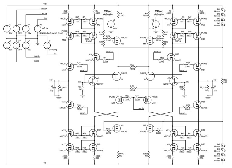
Current Mirror Line Stage
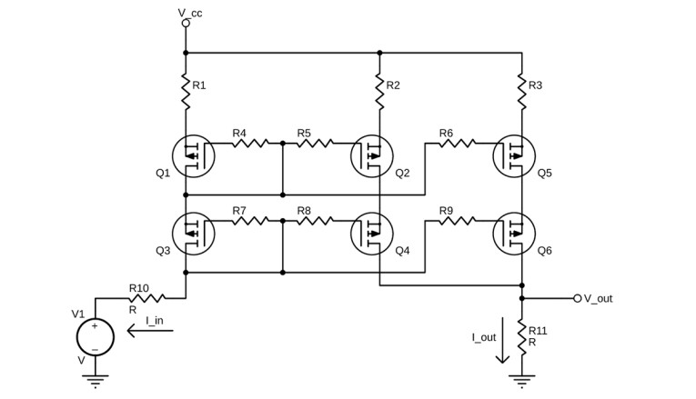
We could also design a Current Mirror Line Stage using a similar technique. The block diagram is shown in Figure 18. In the Current Mirror Line Stage, the input JFETs function the same as they do in the Cascode Line Stage. The difference is that the folded cascodes are replaced by current mirrors. We use cascode current mirrors for accuracy and low distortion. The current mirrors are non-inverting where the folded cascodes are inverting, so the out+ and out- nodes switched sides.
As in the Cascode Line Stage, the input JFETs are cascoded to limit their power dissipation and to keep their drains at a constant voltage for best performance. The output side of the current mirrors are also cascoded for the same reasons.
Here we have to trim the JFET current sources to balance the outputs at 0.00V. This is done by having one set of current sources adjustable while the other set is fixed. The adjustment can be continuous using an op-amp integrator, or manual using a potentiometer. An op-amp integrator will limit the low-frequency response, but we can set the roll-off to well below 1Hz so it has minimal effect on the audio signal path.
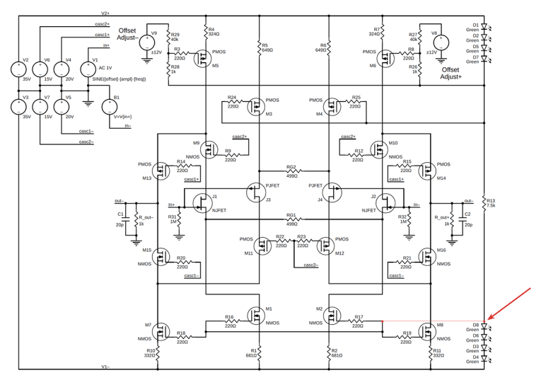
This amplifier, like the Cascode Line Stage is fully differential (balanced) in and out. There are four current mirrors in the Current Mirror Line Stage schematic (Figure 19), a P-Channel Current Mirror for each of out+ and out-, and an N-Channel Current Mirror for each of out+ and out-.
Here again, the input JFETs act as voltage to current converters. The JFET drain currents are loaded by the current mirrors, which reflect the current toward the opposite rail. A P-Channel and N-Channel Current Mirror are combined through cascode transistors to create an output current. The cascode transistors stabilize the voltage at the output of the current mirrors, improving the linearity. The current differences are impressed across the output resistor to create an output voltage.
To control the offset, we have to adjust the current sources. The N-Channel current sources are fixed (M1 and M2), and the P-Channel current sources are adjustable. The adjustment can be made via a potentiometer or an op-amp configured as a non-inverting integrator.
Each has its own advantages, the op-amp continuously trims the offset to 0.000 V, but gives the amplifier a low-frequency roll-off (below 1Hz). The potentiometer setting cannot be adjusted continuously, so there will be a small residual offset at the output, but no low-frequency roll-off.
The resistor values for the current sources in Figure 17 and Figure 19 are dependent on the V(GS) of the MOSFET devices used. These values may have to be modified if different devices are used.
Observations Thus Far
For both of these line stages, I have measured distortion levels of better than -90dB (0.0032%) with 2VPP output, single-ended in and out. At 2VPP, there are no distortion components higher than the third harmonic (3H). At 8VPP out, the distortion is still better than -80dB (0.01%).
My measurement system consists of an HP339A Distortion Analyzer and an HP3580A Spectrum Analyzer. Since most of my consulting work is not related to audio, I cannot justify the expense of an Audio Precision measurement system. I believe the distortion specs previously quoted would be significantly better if measured on an Audio Precision system.
In Part 3, we will discuss some of the details involved in building these line stages including matching transistors, DC servos, and capacitance multiplier power supplies. aX
Read Part 1 of this article here.
Read Part 3 of this article here.
 About the Author
Morty Tarr has more than 30 years’ experience in Electrical Engineering. Morty graduated from Cornell University in 1972 with a Bachelor of Arts in Physics, and a minor in Electrical Engineering. He continued his studies at Tufts University in Electrical Engineering.
Morty began his career at recording studios in NYC and Boston. Then he started to be interested in the design of electronic equipment and made the transition from audio to electronic design. He has extensive experience in the fields of video, audio, test and measurement, networking, and wireless (primarily Wi-Fi and Bluetooth). More recently, from 2006 to 2015, Morty led a team at Bose responsible for advanced development for a $2 billion business. He set the direction for the group and for technology strategy spanning wireless, digital, analog, and system architecture across multiple product lines. Prior to Bose, he worked for LTX developing GHz test systems, at Octave Communications developing conference call bridges, and at Avid Technology. Prior to Avid, at Data Translation, he created the first 24-bit resolution A/D for a PC for Chromatography applications, and then led the team that developed the first Media 100 video editing system. Morty currently has 20 patents and has spent most of his professional career developing first-in-class products. Innovative ideas and new concepts come naturally to him.
This article was originally published in audioXpress, November 2021.