There are two output stage (OPS) types, the DH-220C OPS and the P230 OPS. The P230 adds a third output pair to the OPS. Familiarize yourself with the DH-200/220 and DH-220C designs. Reference the pictures here to see how this new design is assembled. The DH-200 and P220/230 are very similar in construction to the DH-220. This article will refer to the DH-220, but this applies to the other models as well. This is a time-consuming task, take your time, take frequent breaks, and review your work continually and carefully.
When taking on this project, we highly recommended that you have and know how to use an oscilloscope, a signal generator, dummy loads, and a digital multimeter (DMM), but it is possible to build without these. Most DIYers who built the original Hafler units only had a simple analog volt-ohm meter (VOM). The PC-19 from the Hafler kit came pre-assembled and pre-tested. As long as the voltages and currents measure, or can be adjusted to the specifications, and it passes the proverbial smoke test, you can be fairly confident that it should be working okay.
The Bill of Materials (BOM) can be found on the audioXpress online Supplementary Material page. There is a BOM for each of the three PCB types. All parts are in current production, with multiple second sources. Use #18 or #17-AWG solid magnet wire for the coil, L1 (50 cm). The existing coil from the original Hafler board may also be used.
Preliminary Checks
Before you perform the upgrade, it is best to verify that the original amplifier is operating properly. Preliminary things to verify include intact supply fuses, correct supply voltages, absence of significant DC offset at each channel’s output (measured at the binding posts), and secure speaker fuses. Once you are assured of those checks, you can pass an audio signal through each channel’s output, connected to some inexpensive speakers. If you hear distortion-less sound you are good to perform the upgrade. If you have an oscilloscope and a sine wave signal generator, apply a 1kHz, 0.1Vrms sine wave to the input and take the amplifier up to 100W (28.3Vrms) into an 8Ω load.
Visually check the large filter capacitors for signs of leakage or bulging. Replace as required. The original caps in a DH-220 are 2” diameter × 4-1/2” length, with screw terminals, and 10,000µF/75V. If you are upgrading a non-functioning unit, you need to verify that the power supplies work correctly, that it is wired correctly, and that the MOSFETs are functional. Instructions for testing the MOSFETs can be found on the audioXpress online Supplementary Material page.
DH-220 PC-6 or PC-19 and Heatsink Disassembly
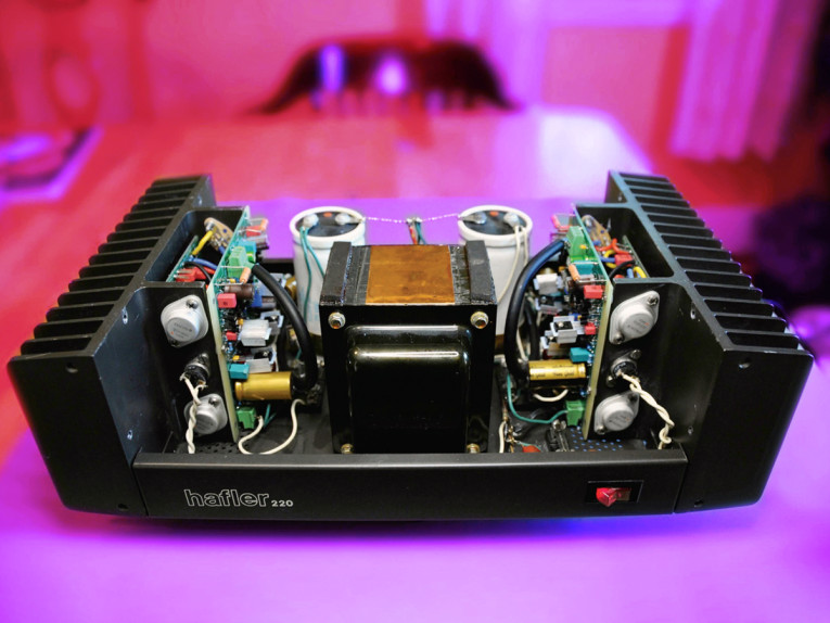
To begin the upgrade, remove the old PCBs from the DH-220. You also need to disassemble the parts between the heatsink ears, since the new OPS will replace them. This includes careful removal of the power MOSFETs and their Mica insulators. Keep track of the locations of the removed parts for each channel; this is one occasion where the camera on your phone comes in very handy! All that will remain will be the MOSFET sockets and the thermal circuit breaker. After removal of the MOSFETs, reattach the sockets with the screws. Carefully clean the old heatsink compound from the heatsinks, the Mica insulators, and the MOSFETS. Do one side at a time.
DH-220C PCB Assembly
It is recommended that you use an electrostatic sensitive device (ESD) bracelet if you are handling the JFETs. Small gauge solder is recommended (0.8mm). For the AFE, if you are using the JFETs in the SOT-23 package, the DIP-6 sockets do not need to be installed. The SOT-23 JFET devices are soldered on the back side, using very thin solder. Inspect them under a magnifier, look for solder bridges. If you are using the leaded JFETs in the TO-71 metal can package, the leads will require forming in order to fit into the DIP-6 sockets. Insert the TO-71 metal can JFETs into the sockets after all the PCB assembly is complete. A SOT-23-6 to 6-pin DIP PCB adapter can also be used.
All resistors that are low wattage can seat on the PCB. Many small resistors are used and all need lead forming. Power resistors (R30, 31, 36, and 50-54) should be lifted off the PCB, ≥1cm, so that air can circulate around them. R1, R2 must be lifted off the PCB by a minimum of 1.5cm to 2cm, as they get very hot.
Coil L1 is easily wound on a 9mm deep ratchet socket. The coil is 11 turns of #17 or #18 AWG magnet wire. Leave some extra wire. You will need to have enough wire so that you can file off the enamel coating to be soldered onto the board. Form the leads for insertion into the L1 position. The existing coil from the original Hafler PCB may be used instead.
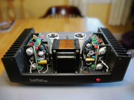
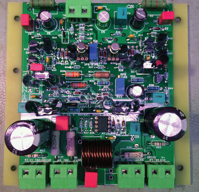
Pre-install the heatsinks on the TO-126 devices, Q17, 18, 20, and 21 before soldering them to the PCBs. Use some Wakefield thermal compound to aid in thermal conduction and insertion. Place a thin layer on the heatsink mating surfaces. When you install these devices, make sure you leave them high enough off the PCB to have enough clearance around them. Check that they are not touching any of the other adjacent components, since they will get hot and need good airflow around them. They are not to be any higher than the height of the big electrolytic capacitors (ecaps) as shown in Photo 1. Be mindful of proper TO-126 device orientation. Place the jumper block on the left two pins of 3-pin header H1, near the silkscreen marking “FOUT.” Install the terminal blocks.
Inspection and Unpowered Testing of the AFE
Inspect every solder joint with a magnifying glass, making sure every device is properly soldered and that there are no cold joints or shorts. Verify correct orientation for every polarized device, including transistors, diodes, ecaps, and the op-amp. Use an ohmmeter to verify that there are no power supply shorts.
DH-220C Output Stage Assembly
The OPS is a simple board to assemble. The PCB sits in between the heatsink ears, riding on spacers. The stiff wires soldered to the MOSFET sockets keep the PCB in position. The use of #18 and #20-AWG stranded copper wire with Teflon insulation is suggested. Smaller #20-AWG wires can be used for MOSFET gate drive connections.
For the wires from the OPS PCB to the MOSFET sockets, use 5cm lengths for the gates and 5.5cm for the drain and sources. Cut, strip, and pre-tin these wires. Use just enough solder to bind the strands, do not blob the solder. For the wires from the AFE to the OPS, use a 5cm wire length for all but the “Sources.” Make them 6cm long. Cut, strip, and pre-tin them. Solder the wires to the extra plated holes for the terminal blocks, on the underside of the AFE.
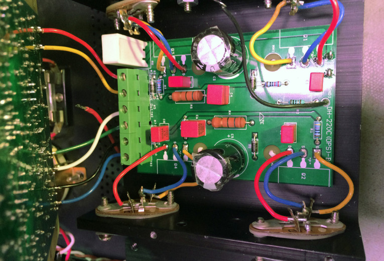
Cut an 8cm piece of black wire, strip, and pre-tin, then solder on the ring terminal to one end. Solder the bare wire end to “GND1” on the OPS board. The ring terminal gets attached to one of the screws on the thermal breaker. This grounds the heatsink for testing of the module when not installed in the chassis without forming a ground loop (Photo 2).
Inspection and Unpowered Testing of the OPS
Inspect every solder joint with a magnifying glass, making sure every device is properly soldered and that there are no cold joints or shorts. Verify correct orientation for every polarized device, including diodes and electrolytic capacitors. Use an ohmmeter to verify that there are no power supply shorts.
Final Assembly
Re-install the power MOSFETs into the same sockets from which they were removed. Apply a thin layer of fresh heatsink compound to the underside of each MOSFET and to the side of the Mica washer that will contact the heatsink. Insert and securely tighten the wires from the AFE into the terminal blocks on the OPS as shown. Attach the OPS ground wire “GND1” ring terminal end to the thermal breaker screw. Replace one of the original keps-nuts (nut with lock washer attached) with a standard 6-32 nut since the ring terminal acts as a lock washer now. Place the original fiber spacers, inserted between the AFE and the heatsink, before fastening the AFE to the heatsink ears, using a 3/16” socket.
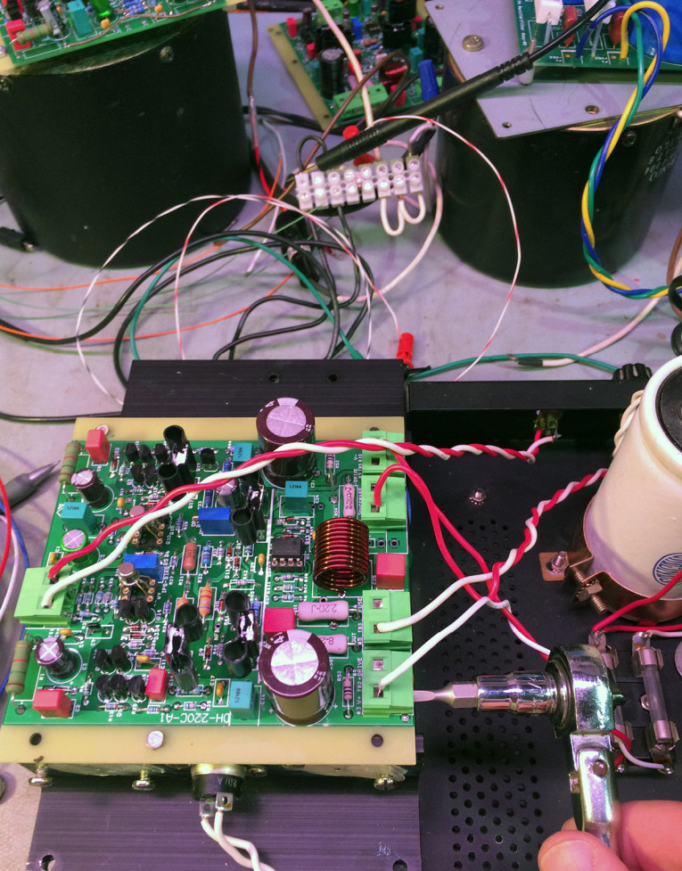
The wires from the rest of the amplifier that connected to the old AFE can be inserted into the terminal blocks (TBs) on the AFE (Photo 3). The wire coming from the “+V” speaker binding post goes to TB3-1, identified as #5 labeled as O/P (Output) on the AFE. The wire coming from the “-V” binding post, goes to TB4-2, identified as #7 labeled as (GND) on the AFE.
AFE Testing
Note, the heatsink, has not yet been mounted to the chassis. Provision is made for testing the AFE by itself, without connection to the OPS. This is strongly recommended. Testing is done by placing the jumper block on the 3-pin header “H1” on the 2 pins on the right side near the silkscreen lettering “TP1”. Don’t forget to put the jumper block back in its normal position before final testing of the amplifier. You can use a separate power supply, if it supplies the necessary ±50VDC to 65VDC or use the supply in the DH-220 chassis. The AFE draws about 55mA for each supply. It will be a bit less when VR1 and VR2 are set for minimum bias.
When performing this standalone/isolated AFE test, place the “H1” jumper in the TP1-NFB position. The MOSFETs should be removed or, if left installed, the ± drive signals to the MOSFET gates are to be disconnected from the AFE and connected to ground. The MOSFET gates should not be allowed to float or be attached to the drive signals. Make sure to insulate any bare leads so they do not short out.
Before applying power, turn the IPS and OPS bias potentiometers VR1 and VR2 to minimum position, counter clock-wise (CCW) using an insulated long shaft small straight blade screw driver or tuning tool. You can use a small jeweler’s screw driver and insulate the shaft with some heatshrink tubing. When you first power up, you can measure the voltage drop across R52 and R53. The nominal current should be around 55mA, so that means you would measure around (55mA × 22Ω) = 1.2V. However, with VR1 and VR2 set fully CCW to their minimum current position, this current will be smaller.
The IPS bias current is adjusted by measuring the voltage drop across one of the four current mirror resistors, R12, 13, and R24, 25. It is specified for a total of 4mA, shared between the two devices in each differential pair. Using some lead clips, attach the leads to one of the chosen measurement points and measure the voltage with the DMM. Adjust RV1 for 360mV across R13 or R25 (180Ω) or 440mV across R12 or R24 (220Ω).
Check the VAS current; the target value is 10mA (±20%). Measure the voltage drop across either R29 or R44 (33Ω). It should be in this range, 264mV to 330mV to 396mV. If it is outside this range, it is okay to adjust the IPS current by ±10% to bring it into range. Reversing one of the JFETs often works. Shunting R9 or R27 with a large-value resistor (e.g., 1kΩ) can also shift the VAS bias current in either direction. Otherwise, refer to the “VAS Bias Current” section in this article or “JFET Matching Procedure” in the audioXpress online Supplementary Material page.
Measure the MOSFET bias voltage, across the ±drive signals, it will range somewhere in the 200mV to 2.7V range depending on the VR2 setting and the MOSFET threshold voltages when the output stage is later connected. Check for proper operation of the VR2 bias control circuit by turning VR2 clockwise (CW) until the bias voltage reaches 1V, then return VR2 to its maximum CCW position. Measure the negative feedback (NFB) DC level at TP1. It should be very close to 0mV, but can be within ±10mV. This offset voltage is controlled by the DC servo.
If you have the necessary test equipment, you can use a signal generator to supply a signal and oscilloscope to view the NFB node to verify that a clean signal is passed through with no signs of oscillation and that symmetrical clipping up close to the supply rail can be achieved. Measure at TP1, with an oscilloscope. Apply a 1kHz, 0.1Vrms sine wave to the input and observe the output at TP1. It should be 2.8Vrms; observe no singing (oscillations). Check the full frequency response; there should be no gain peaking. A 10kHz square wave should exhibit no overshoot or ringing.
Once finished with this initial testing of the AFE, put the “H1” jumper to the normal operational position, (MOSFET sources to NFB) and set the OPS bias to minimum (VR2 CCW) before connecting up the OPS.
Powered Testing with the OPS
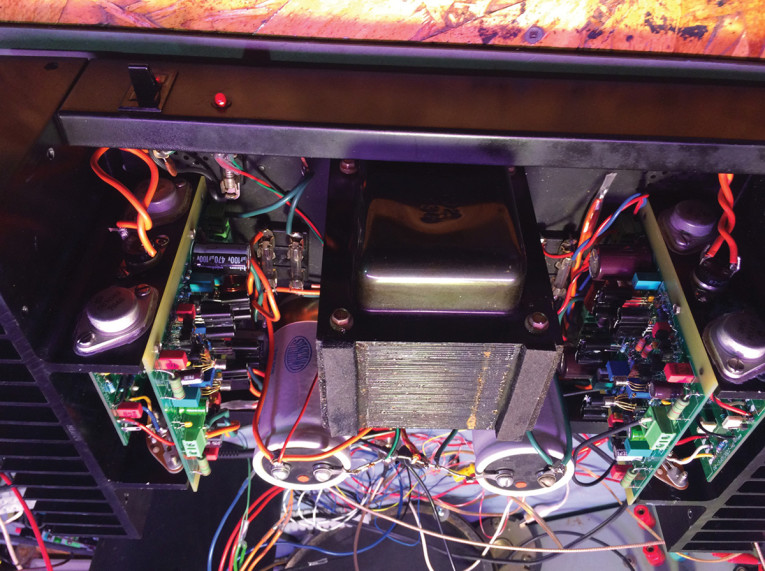
Once the AFE testing is complete, you can wire up the OPS MOSFET gate drive signals as shown in Photo 2. Mount the heatsink assembly to the chassis (Photo 4).
It is best to power up using the Dim Bulb Tester (DBT) initially, just in case there are shorts. A DBT is a device that has an incandescent lamp (~100W to 150W) in series with the AC line. If there are shorts, it might save some devices from damage. Once the power is applied using the DBT, the lamp should be bright initially, but dim down shortly after, as the big filter capacitors charge up. Once done, you can test with full line voltage.
Verify that the output DC offset is less than ±10mV. Using the lead clips, measure the voltage drop at the “BIAS” test points on the OPS. It should be less than 5mV, corresponding to less than 50mA at this time with VR2 set fully CCW. Adjust VR2 CW on the AFE to obtain a reading of 40mV across the test points, corresponding to 400mA. Monitor and let the heatsinks heat up; let the circuit thermally stabilize. Once stable, after approximately 15 to 20 minutes, check/adjust for the 40mV requirement.
If you have the necessary equipment, you can proceed as follows. Apply a 1kHz, 0.1Vrms sine wave to the input RCA jack of the channel being tested and observe the output at the amp out binding post. It should be 2.8Vrms; observe no singing. Check the full-frequency response by sweeping the input, with a 0.1Vrms sine wave, observe no peaking at high frequencies. Adjust the input signal for a 28Vrms signal at the output with no load. Follow this with a quick 8Ω load test. Do these tests for both Left and Right channels. This completes assembly and testing. Enjoy your new amplifier. aX
Project Files
To download additional material and files, visit
http://audioxpress.com/page/audioXpress-Supplementary-Material.html
Go to Part 1 of this article.
About the Authors
 Bob Cordell is an electrical engineer who has been deeply involved in audio since his adventures with vacuum tube designs in his teen years. He is an equal-opportunity designer to this day, having built amplifiers with vacuum tubes, bipolar transistors, and MOSFETs. Bob is also a prolific designer of audio test equipment, including a high-performance THD analyzer and many purpose-built pieces of audio gear. He has published numerous articles and papers on power amplifier design and distortion measurement in the popular press and in the Journal of the Audio Engineering Society. In 1983 he published a power amplifier design combining vertical power MOSFETs with error correction, achieving unprecedented distortion levels of less than 0.001% at 20kHz. He also consults in the audio and semiconductor industries. Bob authored the book Designing Audio Power Amplifiers, published by Focal/Taylor & Francis.
Bob worked at Bell Laboratories, Bellcore, David Sarnoff Research Center and Subcom, where his work has included design of integrated circuits and fiber optic communications systems. Bob maintains an audiophile website at www.cordellaudio.com where diverse material on audio electronics, loudspeakers, and instrumentation can be found.
 Rick Savas has been involved with audio electronics from early on, building Popular Electronics kits and home brew. He attended Centennial College AT&T and earned a diploma in Electronics Engineering Technology 1980. He worked his way up to designing high-density PCBs as used in Gbit/s fiber optic networking systems. He then got back into audio design during his retirement, hooked up with Bob Cordell through DIYAudio, to make some of the designs in his book available for others to construct. Now he is onto the fun stuff—retirement, designing what he likes, and working with talents like Bob Cordell.
This article was originally published in audioXpress, August 2021