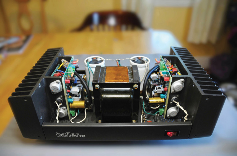
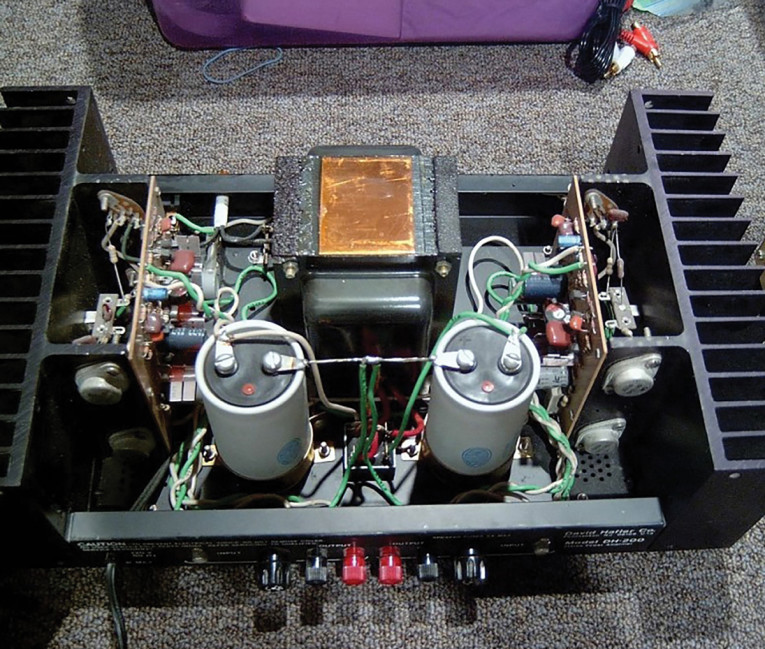
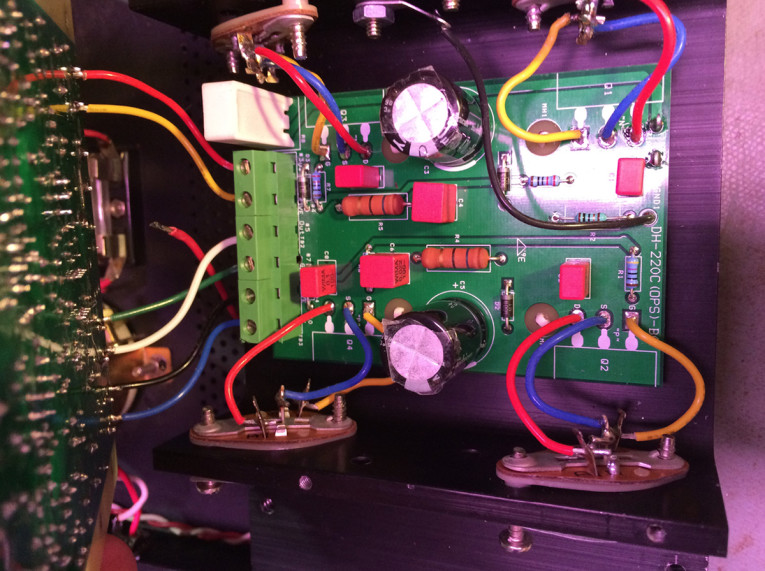
This article describes a construction project for the Hafler DH-220 lateral MOSFET power amplifier (Photo 1). Here we describe the circuit (Part 1) and the assembly (Part 2) of the DH-220C upgrade [2, 3]. The design is implemented on two PCBs, one as a drop-in replacement for the original Hafler circuit board (analog front end, AFE) and the other as a new board (OPS) that consolidates all of the output stage wiring and components within the heatsink and under the main PCB (Photo 2).
This design can also be used to upgrade the Hafler DH-200, DH-500, P225, P230, and P500 amplifiers. A different output board is necessary for the DH-500, P230, and P500 because they employ three pairs of output transistors and have different heatsink profiles. The original DH-220 manual is available for reference [4]. There is also an excellent interview with Erno Borbely, designer of the DH-220 that was conducted by Jan Didden [1].
The design uses most of the original infrastructure of the DH-220, including the chassis, the power supply, heatsinks, and the original output stage power MOSFETs (Photo 3). The amplifier employs two output pairs and is capable of delivering more than 120W/8Ω using the original Hafler power supplies. Each output pair is biased at 200mA for low crossover distortion. The DH-220C incorporates a full-complementary JFET input stage and a push-pull VAS. The design also employs a DC servo for DC offset control [3].
The IPS/VAS
Figure 1 shows the IPS/VAS of the DH-220C. It is a full complementary JFET design using a floating tail [3]. All bipolar transistors in the design are NPN 2N5551 or PNP 2N5401 unless noted.
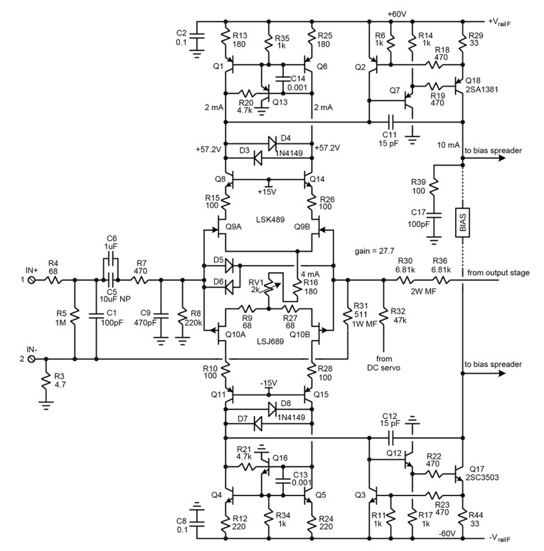
Dual monolithic low-noise N-channel LSK489 and P-channel LSJ689 JFETs are used for the input stage (IPS) [5]. Q9A and B, and Q10A and B form the floating full-complementary IPS, which operates at a tail current of 4mA as determined by trimmer RV1 and R16. RV1 is required to trim the tail current to its design value because of the variability of JFET threshold voltages. Source degeneration resistors R9 and R27 decrease the transconductance of the P-channel long-tailed pair (LTP) to equal that of the N-channel LTP. The JFET LTPs are cascoded to allow for higher rail voltages than the JFETs would otherwise support.
Each LTP is loaded by a current mirror, which includes an emitter follower (EF) “helper” transistor to supply the base current for the mirror transistors. The Vbe voltage drop of the helper causes the differential collector voltages of the cascode transistors to be at the same DC potential because the subsequent VAS also includes an emitter follower. This allows the use of the anti-parallel clamp diodes to limit differential voltage excursions to 1 diode drop. This provides cleaner clipping and also helps prevent over-current in the VAS emitter follower transistor during clipping. The 1N4149 clamp diodes are used because of their smaller capacitance as compared to the popular 1N4148.
Differential loading resistors R20 and R21 help stabilize the VAS bias current. Capacitors C13 and C14 reduce high-frequency interaction between the current mirror and the Miller-compensated 2T VAS by reducing the fT of the helper transistors. Current mirror emitter resistors R12 and R24 are increased from 180Ω to 220Ω, due to slight Vbe differences between the top and bottom VAS circuits.
Input and Feedback Networks
The input network provides AC coupling and two sections of low-pass filtering (LPF) for good EMI immunity. The first LPF section employs R4 and C1. With a 100Ω preamplifier source impedance, it will be down 3dB at about 7MHz. R4 and C1 also serve to form a Zobel network that terminates the interconnect cable at the amplifier end in 68Ω at high frequencies. This is a compromise characteristic impedance for the interconnect cable. R7 and C9 form a second, more conventional input low-pass filter that is down 3dB at about 600kHz.
The feedback network consisting of R31, R30 and R36 sets the closed-loop gain at 28 with fairly low feedback network impedance to reduce noise. The 2W metal film resistors R30 and R36 minimize feedback resistor thermal distortion at low frequencies [3]. The IPS/VAS is intended for use with a DC servo, and the offset correction signal is injected by R32. Input offsets of ±150 mV can be corrected by the servo.
Push-Pull VAS, Bias Spreader, and Drivers
The push-pull VAS comprises a common-emitter stage preceded by an emitter follower that provides high current gain and isolation from Ccb of the CE stage. Q7 and Q18 on the positive side and Q12 and Q17 on the negative side implement the VAS. Quiescent current is set to about 10mA by the voltage drops across the current mirror emitter resistors R13/R25 and R12/R24. These voltage drops in turn depend on the 4mA tail current in the input stage. Q2 and Q3 provide current limiting at about 25mA. In combination with the limited voltage swing from the IPS clamp diodes, VAS transistor base resistors R19 and R22 help limit the current in emitter followers Q7 and Q12 during clipping. C11 and C12 provide Miller compensation to set bandwidth at about 1MHz. Zobel network R39/C17 stabilizes VAS output impedance at high frequencies and suppresses peaking in the open-loop gain response [3].
Figure 2 shows the bias spreader and driver stage. The bias spreader is a CFP design that typically supplies a spread of about 2.7V to bias the lateral MOSFETs and their BJT emitter follower drivers. The CFP bias spreader provides a stiff, low-impedance voltage drop that is advantageous for full complementary designs like this, wherein the VAS bias current can be somewhat more variable than in single-ended designs where the VAS bias current is set by a fixed current source. Trimmer RV2 is used to set the quiescent output stage bias to about 200mA per output pair. The 10-V Zener diodes D9 and D12 provide gate protection and current limiting for the output MOSFETs by limiting their gate voltage with respect to the output rail to about ±10 V. R37 and R40 reverse-bias the Zener diodes by about 2.7V under normal signal conditions to reduce their capacitance.
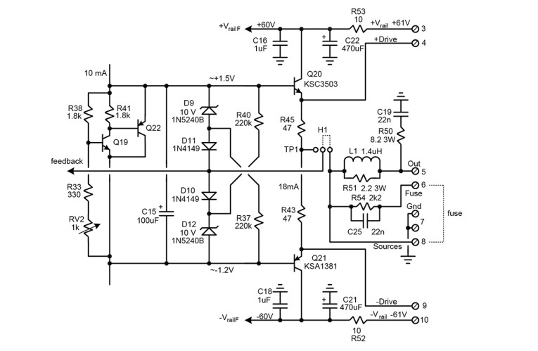
The output transistors are driven by emitter followers that are biased at a healthy 18mA to be able to drive the capacitances of the output MOSFETs with adequate turn-off current even under conditions of fast turn-off. The driver bias resistors provide a center-tap test point TP1 that allows measurement of output stage distortion alone or closure of the feedback loop without the output stage for testing purposes. This feature is implemented by header H1 and its jumper plug. Negative feedback is taken from either TP1 or the MOSFET sources in the output stage.
Output Stage
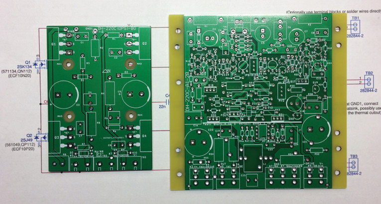
The output stage is on a small PCB that lies underneath the main circuit board within the heatsink area (Photo 4). It replaces the discrete fly-wiring that is used in the original design. It is shown in Figure 3. Gate stopper resistors are included with the same values as used in the original Hafler design. Two Zobel networks effectively in parallel (R4/C6 and R5/C4) allow the stabilizing action to be physically close to each pair of MOSFET sources, minimizing inductance. This also avoids the need for a non-inductive wire-wound resistor, using two 3-W metal oxide film (MOF) resistors [3].
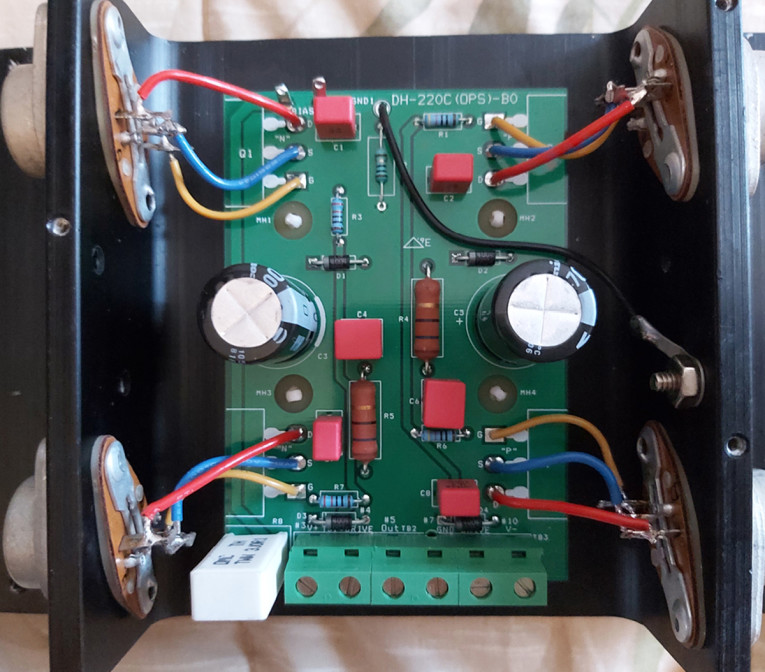
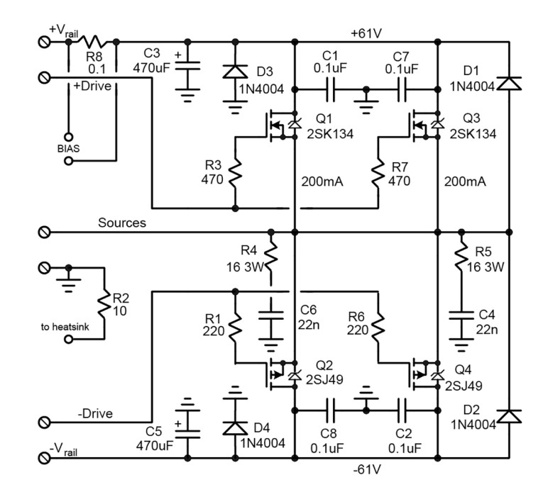
R8 is a 0.1Ω resistor in series with the positive rail to the output MOSFETs. This allows monitoring of the output stage bias current for adjustment. Diodes D3 and D4 protect the amplifier from rail voltage reversal if one rail fails due to a blown fuse. D1 and D2 provide protection against inductive loads causing the output to snap outside the rail voltages. Quiescent current in each of the output transistors is set to about 200mA. This healthy bias extends the “Class-A” region to about 2.5W into 8Ω and helps reduce crossover distortion. The 10Ω resistor R2 connects the circuit ground to the heatsink. This grounds the heatsink when the output module is being tested by itself. R2 prevents the formation of a ground loop when the output module is assembled to the amplifier (Photo 5).
DC Servo
The DH-220C uses a DC servo as shown in Figure 4. The servo can correct up to 150mV of input stage offset. DC servos function to control DC output offset in otherwise DC-coupled power amplifiers. A key advantage of DC servos is the elimination of the negative feedback electrolytic decoupling capacitor.
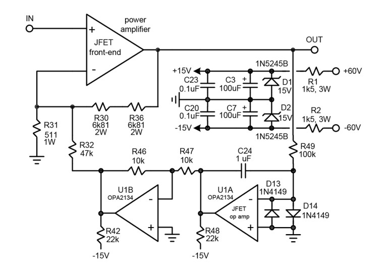
The concept of a DC servo is quite simple. The average DC level at the output is extracted by a low-pass filter, amplified, and fed back to the feedback side of the input stage. This drives the output DC value to zero or a very small value. This permits the use of a low-impedance DC-coupled feedback network while retaining high amplifier input impedance. In practice, an integrator is almost always used to provide both the low-pass filtering function and the gain. This is illustrated in Figure 4 where the input pair of the amplifier is implemented with JFETs. Without the DC servo, output offset would be 280mV with a JFET offset of 10mV.
The amplifier output is applied to a conventional inverting integrator U1A followed by a unity-gain inverter U1B to provide the proper feedback polarity. The integrator is implemented with an audio-quality OPA2134 JFET op-amp to avoid integrator offsets created by input bias current. The servo output from the inverter is applied to the feedback input of the amplifier input stage through a 47kΩ resistor. The DC offset at the output of the amplifier will be approximately the same as the offset of the op-amp, which should be well less than ±10 mV. The low-frequency cut-off created by the servo is at about 0.5Hz.
An audio system signal path often contains more coupling capacitors than necessary. There will usually be one at the output of the preamplifier, and yet another one at the input of the power amplifier. If the power amplifier has a DC servo, the input coupling capacitor of the amplifier can be eliminated, knowing that the DC output of the preamp is probably at or very close to zero. In this case, a further improvement in low-frequency transient response may result by the use of a DC servo. Coupling capacitors C5 and C6 can thus be optionally bypassed. Much more on the design of DC servos can be found in author Cordell’s book, Designing Audio Power Amplifiers [3].
DH-220C Performance
Photo 6 shows the completed board, ready to be tested. The list below summarizes the measured performance of the DH-220C amplifier:
- Power output: 150W @ 8Ω; 260W @ 4Ω; 220W @ 2Ω (< 5 seconds)
- 1kHz THD+N: 0.002% at 120W, 8Ω; 0.0007% at 1W, 8Ω
- 20kHz THD+N: 0.02% at 120W, 8Ω; 0.006% at 1W, 8Ω
- Slew rate: >50V/µs
- Frequency response: 1Hz to 250kHz, +0, -1dB
- Damping factor: >500 from 20Hz to 1kHz; 70 at 20kHz
- 100kHz square wave response: 200ns rise time, no overshoot, into 8Ω
- Capacitive load: stable with all values of capacitance up to 1µF
- Noise with respect to 2.83V output: 104dB A-weighted; 100dB 20kHz un-weighted; 6nV/√Hz.
Figure 5 shows measured 1kHz THD+N vs. power output into 8Ω, 4Ω, 2Ω, and no-load with one channel driven. Using the DH-220 power supply that delivered 56V under load, the amplifier clipped at over 150W and delivered 120W into 8Ω with THD+N of 0.002% at 1kHz. There was no rise of distortion at low power levels that would be indicative of crossover distortion. Dashed lines indicate noise. THD-1 was below 0.0011% in the critical power range between 1W and 10W. THD+N into 4Ω at 200W is only 0.005%, with clipping at 260W. THD+N at 2Ω is still only 0.008% at 200W with clipping at 220W. These measurements were taken with the load connected for less than 5 seconds to obtain the reading; long enough for the power supply to sag and short enough for the transistor junctions not to get too hot.
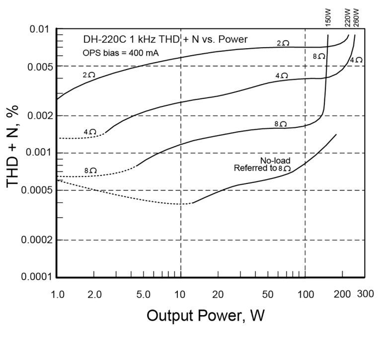
Figure 6 shows measured 50Hz THD+N vs. power. THD+N remains below 0.001% up to 120W into 8Ω, below 0.001% up to 200W into 4Ω, and below 0.002% up to 150W into 2Ω. At 10W, 50Hz THD+N is below 0.0007% for any of these load impedances. Very low distortion at 50Hz, even into a 2Ω load, indicates that this amplifier is capable of high output current and will provide articulate and authoritative bass reproduction. Note that 220W into 2Ω corresponds to peak output current of 14.8A. Thus, the amplifier is adept at driving difficult loudspeaker loads.
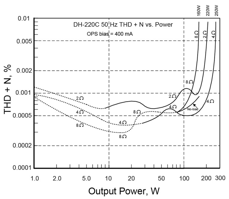
Figure 7 shows measured 20kHz THD+N versus power. THD+N remains below 0.02% at 20kHz up to 120W into 8Ω. In the critical region below 2W it is only 0.006%. Clipping occurs at 150W with THD+N of 0.2%. Even at 200W into 2Ω, THD-20 is only 0.12%.
THD increases from 1kHz to 20kHz as feedback loop gain decreases, as expected.
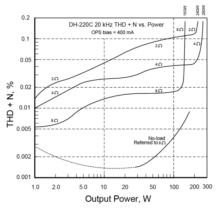
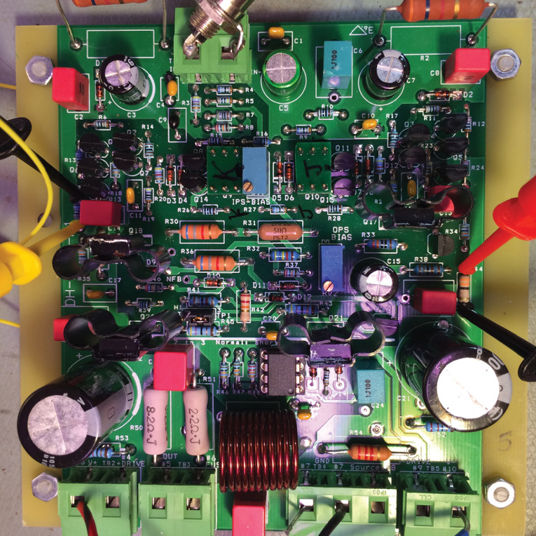
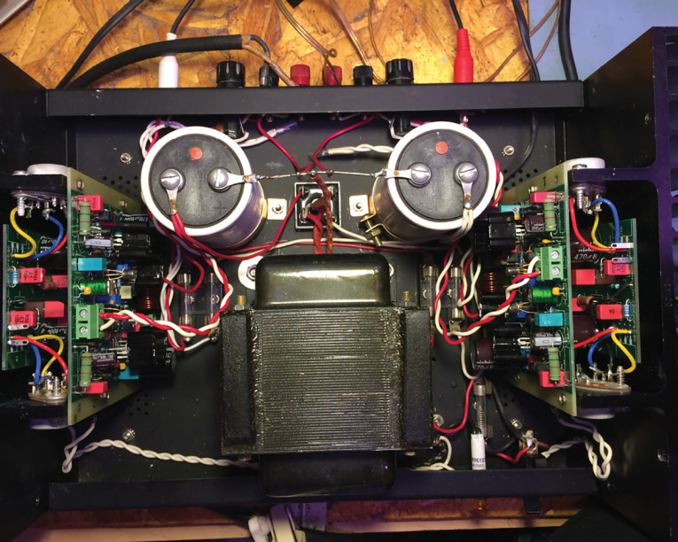
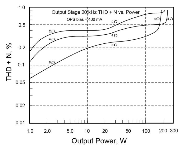
Photo 7 shows the PCBs in place, ready for the final test. Figure 8 shows measured 20kHz THD+N vs. power for the output stage alone. This shows that output stage distortion dominates, and comparison with Figure 7 allows one to see the reduction due to negative feedback around the output stage. THD+N is about 0.3% into 8Ω at 100W, about 0.5% into 4Ω at 200W and 0.8% into 2Ω at 180W. THD+N for the output stage varies little with frequency.
Summary
The DH-220C provides an upgrade path for the original Hafler DH-220 that includes a full-complementary JFET input stage and a DC servo, among other circuit improvements. Reduced EMI susceptibility has also been implemented in the design. A separate output board consolidates and replaces the discrete wiring employed in the original Hafler design and places decoupling capacitors and the Zobel network closer to the output transistors, improving stability and reducing radiated nonlinear magnetic fields that can introduce distortion into the input stage.
Part 2 of this article
In Part 2, detailed assembly and testing will be described. Printed wiring boards are available for this project, as are pre-soldered LSK489 and LSJ689 dual JFETs in SOT-23 packages. The PCBs can be found on eBay with or without the JFETs. More information is available for purchasers of the PCBs. Additional information can also be found at http://cordellaudio.com [6].
Read Part 2 of this article.
References
[1] J. Didden, “The Borbely Annals,” MultiMedia Manufacturer, September/October 2008,
[2] B. Cordell, “The DH-220C Audio Amplifier Design,” Presented at Burning Amp 2016,
www.youtube.com/watch?v=V7-27fDgqco
[3] B. Cordell, Designing Audio Power Amplifiers, Second Edition, Routledge/Focal Press, 2019.
[4] Hafler DH-220 user manual,
https://hafler.com/pdf/archive/DH-220_amp_man.pdf.
[5] Linear Integrated Systems LSK489 and LSJ689 datasheets, www.linearsystems.com.
[6] Cordell Audio website, http://cordellaudio.com
This article was originally published in audioXpress, July 2021.
About the Authors
 Bob Cordell is an electrical engineer who has been deeply involved in audio since his adventures with vacuum tube designs in his teen years. He is an equal-opportunity designer to this day, having built amplifiers with vacuum tubes, bipolar transistors, and MOSFETs. Bob is also a prolific designer of audio test equipment, including a high-performance THD analyzer and many purpose-built pieces of audio gear. He has published numerous articles and papers on power amplifier design and distortion measurement in the popular press and in the Journal of the Audio Engineering Society. In 1983 he published a power amplifier design combining vertical power MOSFETs with error correction, achieving unprecedented distortion levels of less than 0.001% at 20kHz. He also consults in the audio and semiconductor industries. Bob authored the book Designing Audio Power Amplifiers, published by Focal/Taylor & Francis.
Bob worked at Bell Laboratories, Bellcore, David Sarnoff Research Center and Subcom, where his work has included design of integrated circuits and fiber optic communications systems. Bob maintains an audiophile website at www.cordellaudio.com where diverse material on audio electronics, loudspeakers, and instrumentation can be found.
 Rick Savas has been involved with audio electronics from early on, building Popular Electronics kits and home brew. He attended Centennial College AT&T and earned a diploma in Electronics Engineering Technology 1980. He worked his way up to designing high-density PCBs as used in Gbit/s fiber optic networking systems. He then got back into audio design during his retirement, hooked up with Bob Cordell through DIYAudio, to make some of the designs in his book available for others to construct. Now he is onto the fun stuff—retirement, designing what he likes, and working with talents like Bob Cordell.