
- on Project Articles
- Article
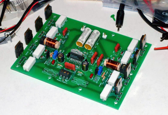
High End 120W MOSFET IC Driven Amp - Extra notes
Extra notes from the author - Reader’s Letters.
Questions about the project
1. Unless the amplifier is powered from a 240V line, it is against NEC to switch both input lines. The grounded neutral on a 120V line may not be switched (or fused). UL will not list a device with a switched neutral.
2. How does the power supply provide ±56V from a 44VCT winding on T1? 88VCT would work.
3. The Fig. 2 schematic shows device U1 as a loudspeaker. The parts list identifies the LM4702 as U1. Where does the lead connected to R13, R3, L1 actually go?
Charles Stillhard - Bisbee, Ariz.
Jack Walton responded:
1. As a ham radio operator for many years, I posed this concern to the technical experts at the American Radio Relay League in Newington, Conn. Reader Stillhard is correct. In 120V AC lines (“Hot Neutral Ground”) the ground should not be fused or switched, which can pose a shock hazard. In 220V AC lines (“Hot Hot Neutral”) both lines may be switched.
2. Each side of the center-tapped transformer I used delivers approximately 44V AC. After rectifying and filtering, and given the losses in the surge protectors and diodes, this averages out to somewhat less than the theoretical value you would expect.
3. I am sorry for the confusion with respect to the connection of the driver board and the output board. The U1 and U5 designations are the same device. While a loudspeaker schematic symbol is shown, in actuality this is just to illustrate where the speaker should be hooked up. The node that joins the “load sharing” resistors on the output board (R3-6) is the same one that conjoins L1, R1, R3, R13.
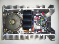
4. I lifted a page from the work of Erno Borbely (“New Power Amp Modules, Parts I and II,” Audio Amateur, 3 and 4/93) and decided that a more flexible layout would use separate driver and output boards, allowing for bipolar transistors or MOSFETs in the final stage. A board for the output stage is not really necessary; just keep in mind, however, that the gate stopper resistors should be as close to the MOSFET gate as possible.
It seems there is an error in Fig. 2 of Jack Walton’s article. I believe that C13 (the 470nF negative power supply bypass cap) should be connected to the side of R16 nearest the LM4702.
Keith Levkoff
kLevkoff@panix.com
Jack Walton responds:
As reader Levkoff correctly points out, capacitor C13 is connected directly to Vee pin of the LM4702. The connections are correct on the printed circuit board, incorrect on the schematic.
The Gerber Files for the driver board have been posted to the aX website (www.audioXpress.com) along with images of the top and bottom copper layers and silkscreen. These files and images are for Version 1.4 boards. The easiest way to get started is to use the images (which were produced at 100%) and print onto 3M transparency film.
Subsequent to publishing the article, I had some observations for improving the performance beyond the statistics published at the end of the article:
1. Before installing the RC network consisting of R2/C14 (330Ω, 10pF), check to see whether the amplifier actually oscillates. If there is no problem with oscillation, you can leave out these components and the THD% improves by a hair.
2. On the output stage schematic I showed 330pF capacitors (C1, C3) connected from gate to source of the output MOSFETs. If you eliminate these capacitors, the slew rate of the amplifier will decrease, but stability will be enhanced. Your mileage may vary depending upon the load characteristics and the precise configuration of the output stage. In the amplifier I used for my day-to-day listening, C1/C3 are in place, but the R2/C14 RC network is disconnected.
After the article was published, Troy Huebner of National Semiconductor wrote an application note which is required reading: “LM4702 Driving a MOSFET Output Stage,” AN-1645. In particular, Huebner demonstrates an output biasing scheme for the Renesas Lateral MOSFETs which simply consists of a 1K potentiometer across the source and sink pins of the LM4702 and a 47K resistor from sink to ground. He also uses 10pF capacitors (which I show as 30pF silver micas, C4 and C11 on the output stage) which “hot up” the slew rate of the AN-1645 amplifier. I have used this simpler bias scheme which works well.
Huebner further describes the method for explicitly determining the value of gate stopper resistors. Use of other output devices, such as the Vishay IRFP240/9240, Magnatec BUZ901/906, and Toshiba 2SK1530/2SJ201 MOSFETs, are described in this application note. National promises an application note that will discuss the optimization of the LM4702 compensation capacitors.
Version 1.6 driver boards, the 2SK1058 and 2SJ162 lateral MOSFETs, and some of the ancillary bits and pieces are available on my webstore, www.tech-diy.com/LM4702_Kits.htm. The amplifiers based upon the LM4702 are very listenable, and I am gratified by the enthusiastic response to the article.
Further instructions:
http://www.tech-diy.com/Amplifiers/IC_DriverCircuits/LM4702/LM4702_Instructions.pdf
http://www.tech-diy.com/Amplifiers/IC_DriverCircuits/LM4702/LM4702_Driver.htm
About the author
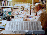
Jack Walton is an investment consultant and entrepreneur in Short Hills, NJ. His educational background is in chemistry, physics, and finance. He has had a lifelong interest in electronics, ham radio, photography, and the arts.
Attachment