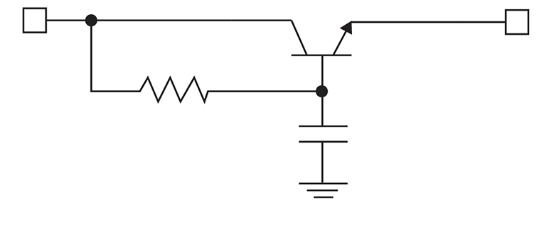
The circuit in Figure 1 is mentioned in “analog circuit cookbooks” and websites as a “capacitance multiplier” and is useful as a power supply low-pass filter (see Figure 1). It is commonly said that, like Miller capacitance, the capacitor’s value in this circuit is “multiplied” by the transistor gain (β) to lower the filter’s pole frequency.
The transistor-enhanced filter does that and more. Here is an explanation of how the transistor lowers the filter’s insertion loss and pole frequency.
Analog Circuit Design
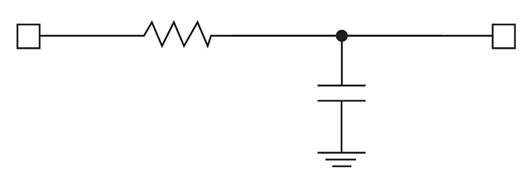
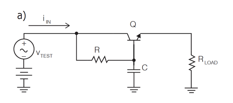
The raison d’être for this circuit is that the voltage drop and power dissipation across the resistor in a simple RC low-pass filter is too great for most low-voltage supplies (see Figure 2). A Zener diode is often added to the transistor-enhanced low-pass filter in parallel to the capacitor to regulate the output voltage.
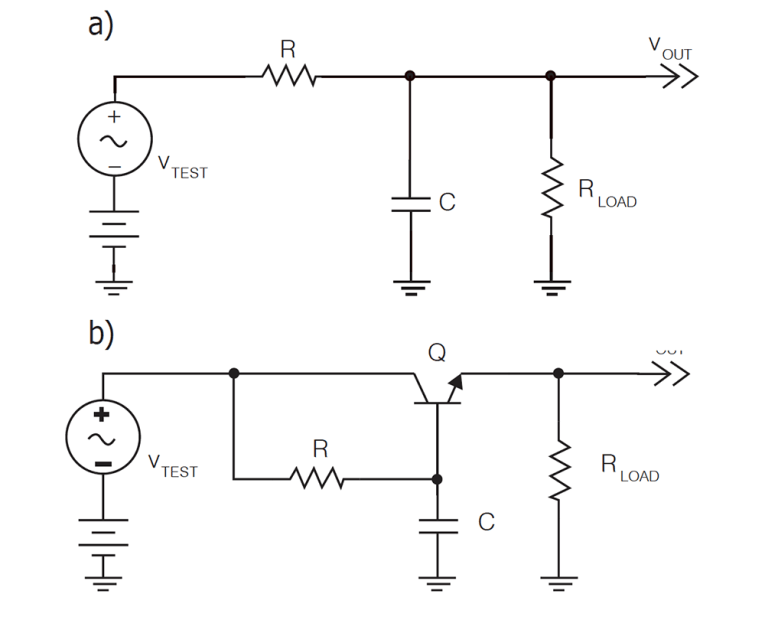
But for the time being, let’s examine the filters themselves. Figure 3 shows both circuits used as power supply filters. We can understand how both these filters behave by calculating their voltage transfer functions, input impedances, and output impedances.
At this point, I’d like to stress the importance of putting pencil to paper when designing analog circuits. SPICE simulations and hardware breadboards are excellent verification methods, but a derived equation gives you two important things: performance sensitivity to component values and an intuitive understanding of how the circuit works. The goal of hand analysis should not be to determine exact answers (because this is impossible), but to derive approximate solutions that provide insight into how the circuit works. These simple circuits are good practice for developing your analysis technique.
In the following derivations, I’m assuming you know the basics of transistor small-signal analysis and the concept of Laplace transforms.

Voltage Transfer Function
To calculate a voltage transfer function, maintain all the DC bias voltages and currents, apply an AC test voltage (VTEST) to the circuit’s input and calculate the circuit’s AC output voltage (VOUT). The voltage transfer function, which shows how the AC output voltage is a function of the AC input voltage, is a function of frequency and equals VOUT/VIN.
Because we are working in the frequency domain, we use Laplace transform versions of impedances and transfer functions; the Laplace variable(s) represents frequency dependence. Figure 4 shows the circuit setups for calculating voltage transfer functions for both the RC filter (see Figure 4a) and the transistor-enhanced RC filter (see Figure 4b). Note that for these calculations we are assuming the power source’s output impedance is negligibly small relative to the filter and load impedances.
For the RC filter, we can use the voltage divider equation to calculate VOUT/VIN.
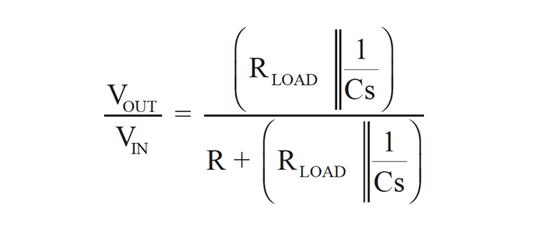
Some algebraic manipulation puts the transfer function in “pole/zero form:”
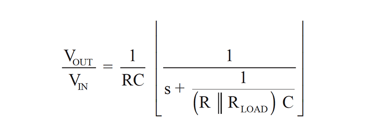
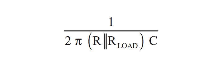
From this equation, we can see that the filter’s pole frequency (in Hertz) is:
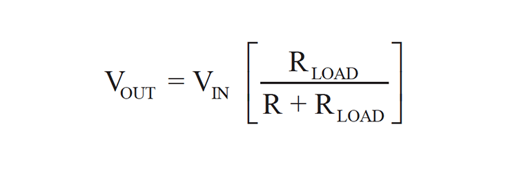
At low frequencies (s→ 0), the capacitor is open circuit and the resistors form a voltage divider. Thus:
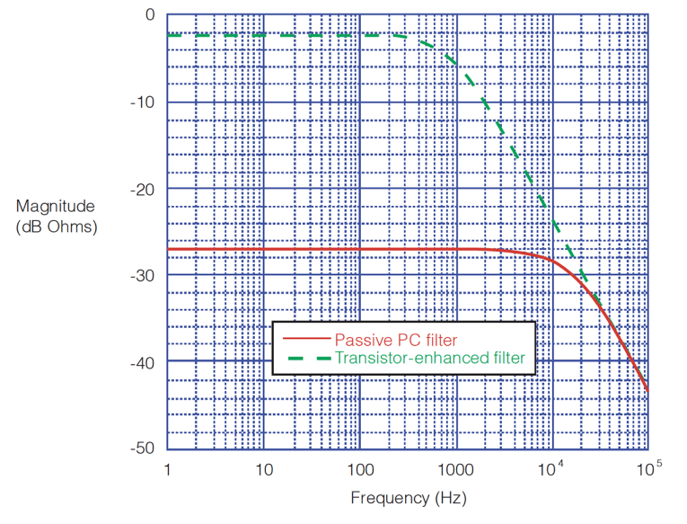
At high frequencies (s→ ∞), VOUT goes toward zero because the capacitor shorts across the load. Graphically, the magnitude (in decibel ohms) of this transfer function is shown in Figure 5. We can use a simple bipolar transistor small-signal model (described in many texts), as shown in Figure 6, to calculate an approximation of the voltage transfer function for the transistor-enhanced circuit in Figure 4b.
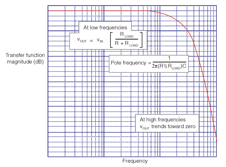
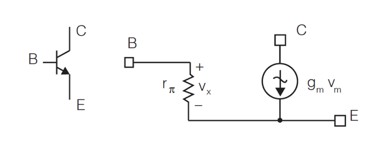
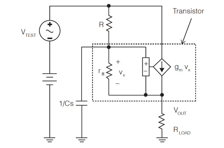
Figure 7 shows the small signal circuit setup for calculating the approximate voltage transfer function of the transistor-enhanced low-pass circuit in Figure 4b. This voltage transfer function can be obtained by setting up and simultaneously solving two equations. The first is that the voltage VOUT is equal to the currents flowing through the load times the load resistance.

The second equation is obtained by summing currents using Kirchoff’s current law at the transistor’s base.
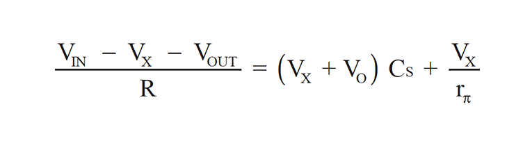
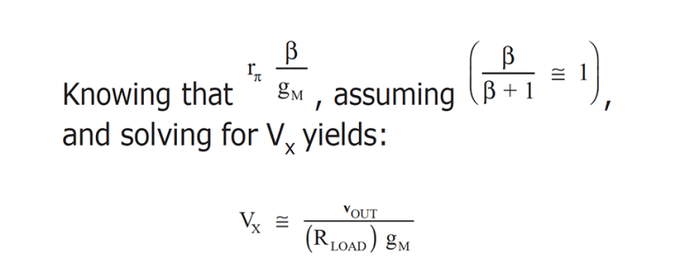
Substituting the first equation into the second, solving for VOUT/VIN, and neglecting small terms yields:
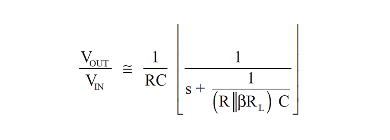
This equation is an excellent approximation of the actual voltage transfer function, if you have a reasonable idea of your transistor’s β. From this transfer function, we can see that the transistor-enhanced filter’s pole frequency is:

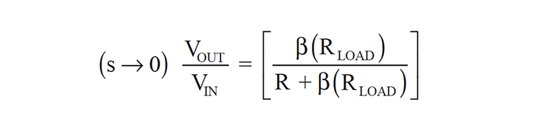
At low frequencies (s→ 0)
At high frequencies (s→ ∞) and VOUT goes toward zero. Figure 8 shows graphically the difference between voltage transfer functions for a simple RC filter and a transistor-enhanced circuit's transfer function with the same component values (R=1,000Ω, C=0.22μF, RL=47Ω). Comparing the two transfer functions, we can see that the benefits the transistor-enhanced filter offers (a lower pole frequency, which results in better ripple rejection, and lower low-frequency insertion loss, which results in a lower power dissipation and lower drop out voltage) are more effective than equivalently multiplying the capacitance by the transistor’s β.
The reduced low-frequency insertion loss is equivalent to dividing the filter resistance (R) by β, and the lower pole frequency is equivalent to simultaneously multiplying the capacitance (C) by β and dividing the filter resistance (R) by β.
Input Impedance
To calculate a circuit’s input impedance, leave the circuit output open and apply an AC test current (ITEST) or test voltage (VTEST) to the circuit’s input and calculate the circuit’s AC input voltage (VIN), or input current (IIN), respectively. The input impedance is VIN/ITEST, as a function of frequency.
By inspection, the RC filter (see Figure 4a) input impedance is:

Working out the algebra yields:
This impedance has a zero, at a frequency of:

and a pole at a frequency of:

At low frequency (s→ 0), when the capacitor is high impedance, the input impedance becomes R+RL and at high frequencies (s→∞), when the capacitor is a short-circuit, the impedance is R. Figure 9 shows the circuit schematic and the simplified small signal model used to calculate the transistor-enhanced filter’s input impedance.
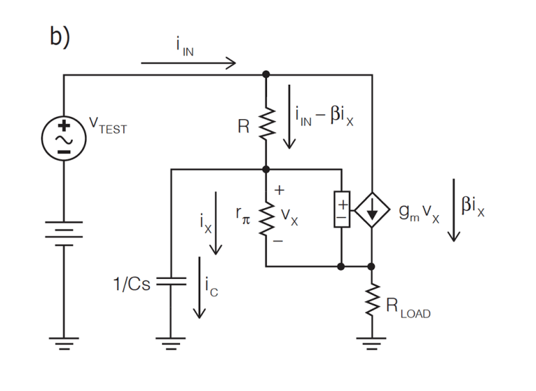
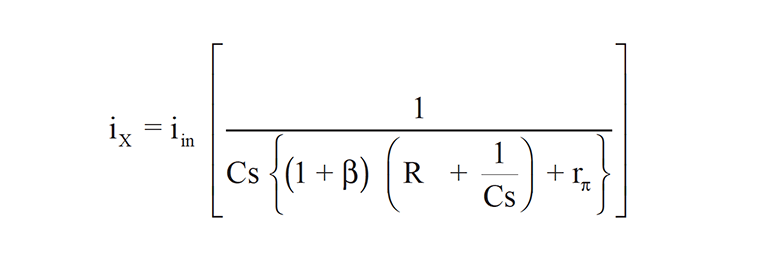
In this case we’ll apply an AC test voltage (ITEST) to the circuit’s input and calculate the AC input current (IIN). To find the input impedance, we need to solve two Kirchoff voltage law equations. The first is that the voltage across the capacitor (equal to the current flowing through the capacitor times the capacitor’s impedance) plus the voltage across the resistor (equal to the current flowing through the resistor times its resistance) equals the test voltage.

The second equation is that the voltage developed across the capacitor is equal to the voltage developed across the load and rπ.
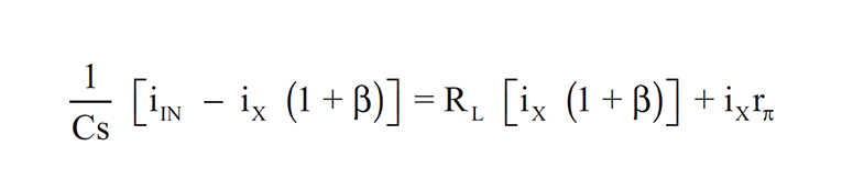
This equation can be solved for Ix as a function of IIN.
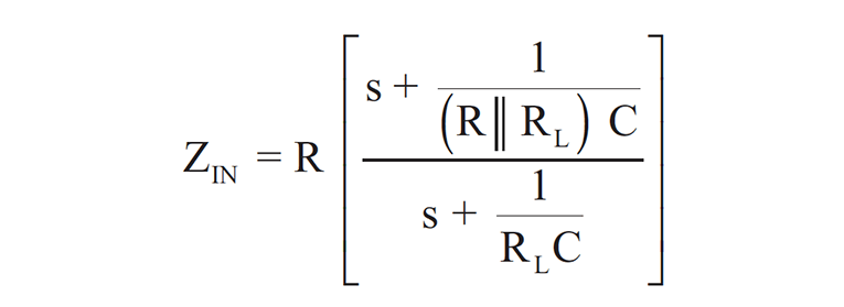
This equation can be substituted into the first equation, and (after some algebra) solved for the input impedance (VTEST/IIN). If we assume βRL>>rπ, which is a reasonable assumption for a power supply filter because the current through the transistor should be relatively large (and thus rπ should be relatively small), the input impedance is approximately equal to:
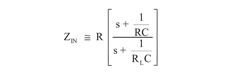
Comparing this to the input impedance of the simple RC filter shows that, although at high frequencies (s→∞) the input impedance of both circuits approaches R, at low frequencies (s→ 0) the passive RC filter’s input impedance approaches R + RL while the transistor-enhanced filter’s input impedance approaches RL. When using the passive RC filter, at low frequencies the power source has to feed the filter resistance (R) in series with the load, but, when presented with the transistor-enhanced filter, the power source feeds only the load at low frequencies. In addition, the transistor-enhanced circuit presents a high impedance to higher-frequency power line ripple.
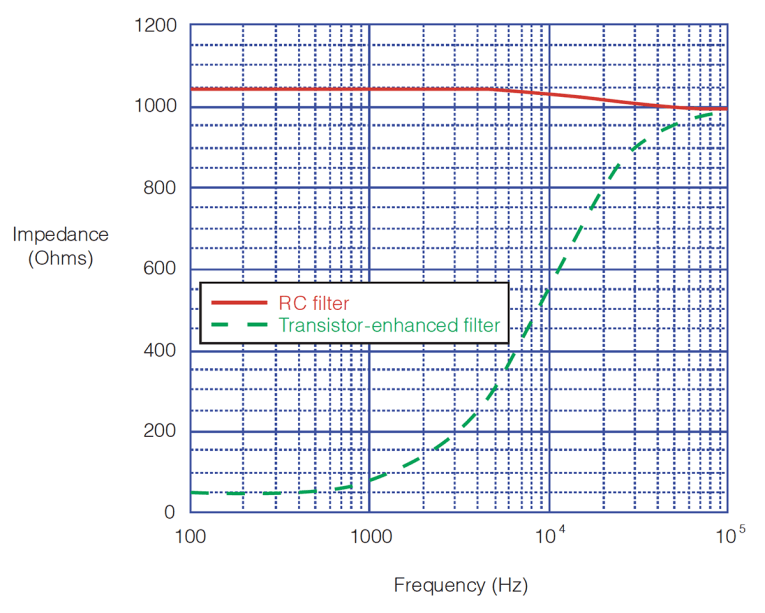
Figure 10 is a comparison plot showing the input impedance magnitudes of a simple RC filter and a transistor-enhanced filter. For both circuits, R = 1,000Ω, RL = 47Ω, and C = 0.22μF.
Output Impedance
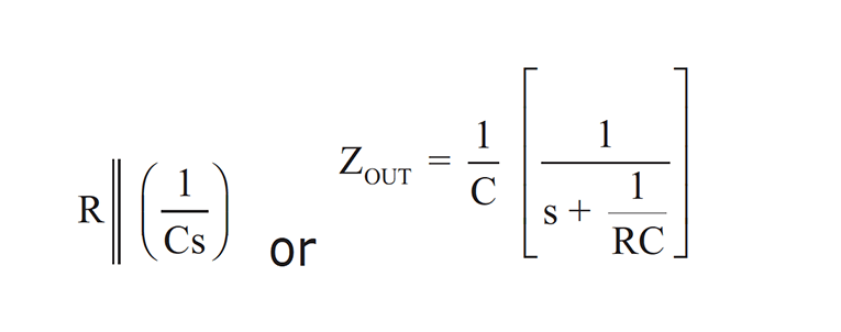
By inspection, the output impedance of the passive RC filter is:
Note that the load resistance is not included in the output impedance calculation. To calculate the transistor-enhanced filter’s output impedance, ground the circuit input, apply an AC test current (ITEST) or test voltage (VTEST) to the circuit’s output and calculate the circuit’s AC output voltage (VOUT), or output current (IOUT), respectively.
The output impedance is VOUT/ITEST, as a function of frequency. Using the same small-signal transistor model as before, the transistor-enhanced filter’s output impedance can be found to be approximately.
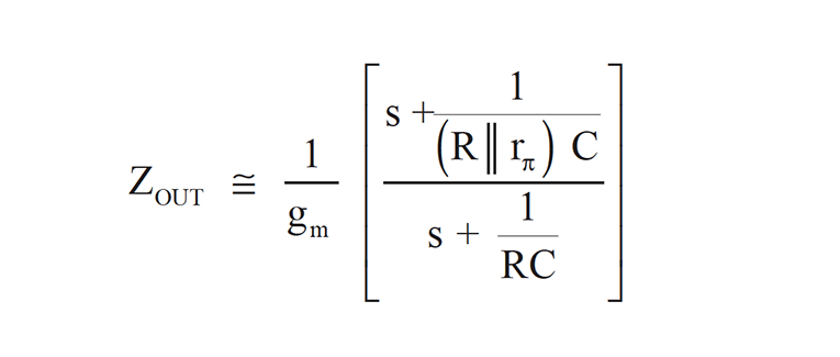
This is approximately equal to:
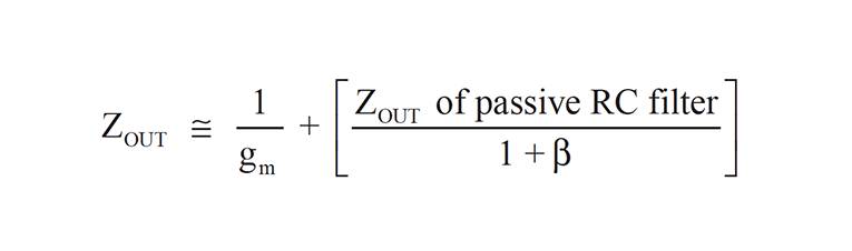
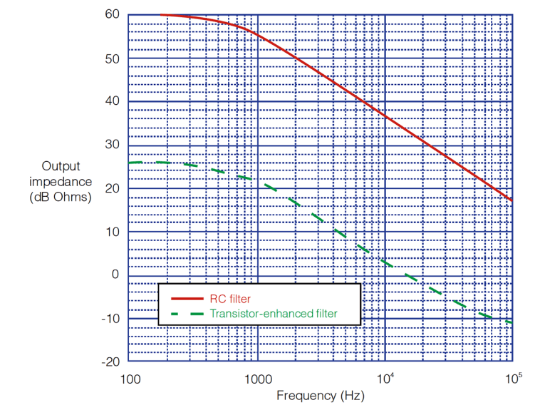
Figure 11 shows a comparison plot between the output impedance magnitude (in decibel ohms) of a simple RC filter and a transistor-enhanced filter.
Note that the transistor-enhanced filter reduces the output impedance by β, and at high frequencies, the transistor-enhanced filter’s output impedance approached 1/gm. When using the transistor-enhanced filter, be sure to bypass its output with capacitance to lower its high-frequency output impedance.
In summary, we can see that the transistor-enhanced filter’s benefits are more effective than equivalently multiplying the capacitance by the transistor’s β. Adding the transistor provides two advantages over the passive RC filter. It lowers the insertion loss, and thus, there is less voltage drop and lower power dissipation across the filter. It also lowers the pole frequency, which is equivalent to simultaneously multiplying the capacitance by β and dividing the filter resistance by β, for better ripple rejection. aX
This article was originally published in audioXpress, August 2012.
 About the Author
Bill Reeve has a life-long interest in electrical and mechanical design. He has Masters of Science degrees in Electrical Engineering, Mechanical Engineering and Geological Engineering. He worked first as a consulting geologist, then spent 28 years at Lockheed Martin as a program director managing the development of NASA satellites and space instruments, in addition to serving as an Engineering Director at the DeWalt Industrial Tool company. When he retired from Lockheed Martin, Bill was recruited by Google to manage large projects, where he is currently Technical Program Manager.