The normal A2B data rate is 49.152 Mbps. As noted in th first part of this article series, we are rounding the data rate up to 50 Mbps. This data rate corresponds to a 49.152 MHz fundamental frequency, which is also rounded off to 50 MHz.
ADI offers a number of IC variants that are cost optimized for particular use cases. The AD2428, which supports the entire feature set, will be the part chosen for most designs. We are using the AD2428 part number to stand in for any of the variants, with the understanding that features and circuits may need modification for the other versions. While the features are discussed in the context of the automotive use cases, we are also considering use cases anywhere consumer, commercial, or pro audio devices may be found.
A2B Bits at the Wire Level
The basic interface for the ADI transceivers is Low Voltage Differential Signaling (LVDS), with some differences in the details. Released in the mid-1990s, LVDS is used in many applications to move digital data over high speed serial links [1]. As with balanced audio, two lines 180° out of phase with each other are used to send data. This increases noise immunity, and in the case of high-speed digital signals, minimizes radiated electromagnetic interference (EMI) when used with twisted pair wire compared to single-ended configurations.
Another consideration for digital signals, which at the frequencies involved are better thought of as radio frequency (RF) vs. 1s and 0s, is impedance matching. At audio frequencies impedance is generally only important in terms of maximizing voltage transfer (audio interconnects). At radio frequencies, impedance mismatches cause signal reflections, resulting in distorted waveforms and increased EMI. Users of AES/EBU or SPDIF interfaces, which are only a few megahertz, have no doubt seen required impedance statements in datasheets. At the (nominal) 50 MHz A2B frequencies, particularly with longer wire lengths, impedance matching becomes part of the must-haves to correctly move data around.
LVDS only describes an electrical interface, not what it is used for. In the case of A2B the data is Manchester encoded, which allows the receiving end to easily recover the clock needed to know where the bits are. Manchester encoding encodes data on clock edges, rising for a 0 and falling for 1. Therefore instead of trying to determine the signal level at a specific instant in time, the receiver only needs to know the before and the after state—an easier proposition for which to build hardware. Manchester encoding is DC balanced, meaning systems can be AC coupled, which in turn simplifies phantom power design. It’s also easy to extract a clock from.
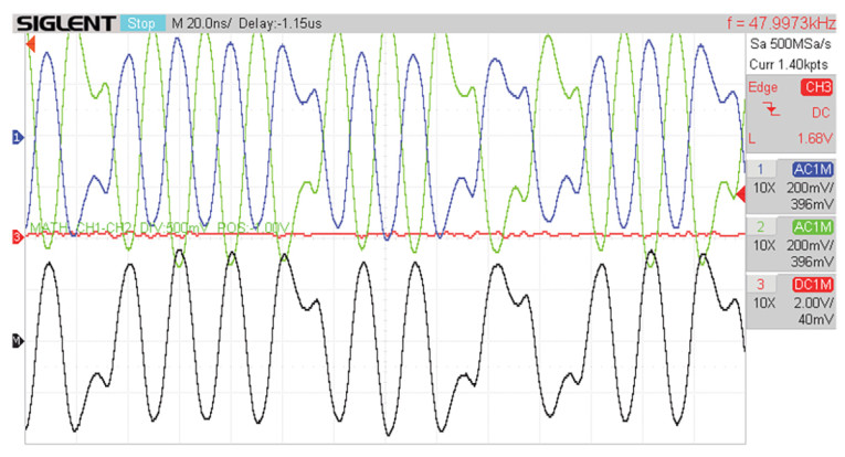
Figure 1 shows an actual waveform captured from hardware. Though not captured on a very wide bandwidth scope (200 MHz in this case) with specialized differential probes (you know, the ones that cost more than your last car), we want to illustrate what actual waveforms look like.
Also of interest in understanding A2B is the spectrum of the signal, as shown in Figure 2. The peak is at the expected (approximately) 50 MHz and third harmonic at 150 MHz. The spike close to 100 MHz is actually a nearby FM station and illustrates the importance of knowing your test tools and system, otherwise one might assume in this case there’s some sort of bad 2× clock signal ending up on the wire.
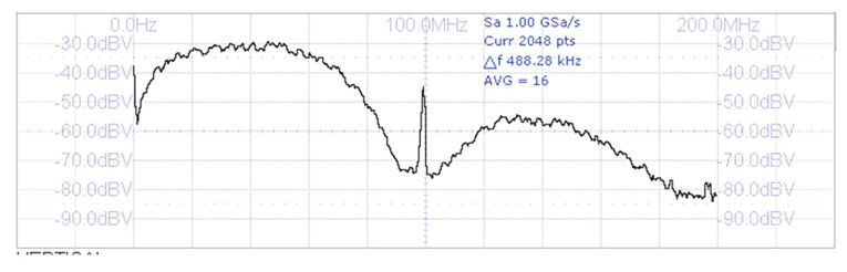
The peak is broad as the data causes differing patterns — the theoretical spectrum can be calculated from the signal properties but that is beyond what we need to know to use A2B. Below a few megahertz, there’s not much signal energy, which will be helpful in understanding the filter components used in the ADI recommended circuit.
We can also start to understand the cable length limitations are not just a question of drive strength. The master node needs to send downstream all of the data (1024-bit periods are allocated per 48 kHz frame, one bit period is therefore 20.3 nsec) and receive all of the upstream data back within 20.83 µsec. Cat 5 propagation delay is about 5 nsec/m. The 40 m length limit corresponds to a delay of 200 nsec in each direction, or 400 nsec total — about 20-bit periods.
Each node also has to receive the data and reclock it out again and the nominal time for that is 9-bit periods. With 10 nodes that totals 180-bit periods. Between cable delay and node delay about 200-bit periods are needed to deal with delays related to the physics of the problem, leaving about 800-bit periods for headers, control information, and audio data. Those bit periods are allocated between the up and down stream directions.
A2B Analog Sections
With high-speed digital signals as well as analog RF signals, the source and load impedance must be matched [2]. Many differential digital systems use a 100Ω impedance with twisted pair wire (e.g., a CAT5) can easily meet that requirement in a low-cost manner. While a single 100Ω resistor at the IC input meets the matched termination requirement, most designs will use two 50Ω resistors with the center connection AC grounded via a large value capacitor. This improves common mode rejection (CMR) and has no DC current draw—the details of the advantage of this scheme can be found in the prior reference.
Standard LVDS is normally unidirectional and A2B operates bidirectionally, which means termination resistors need to be on each end of the cable to accommodate data being sent in both directions.
Figure 3 shows the circuitry recommended by ADI. This drawing does not include the parts to extract phantom power from the bus, as well as other parts needed for local powered slaves. Full details are available from ADI [3]. Manchester encoding ensures no DC, therefore the system can be capacitively coupled. The two 10 nF capacitors serve that purpose; at 50 MHz XC < 0.3 Ω, and we can treat them as a piece of wire as far as the data signal is concerned. In this discussion, we’ll ignore the DC offset needed by the AD2428 A2B transceiver.
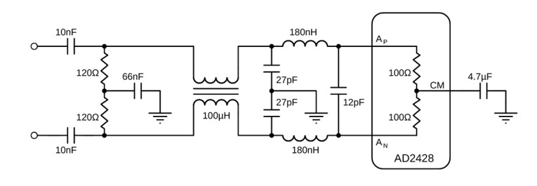
The first thing the astute reader probably noticed is two 120Ω termination resistors and said “wait, you just told me the termination impedance is supposed to be 100Ω.” And indeed it (sort of) is. The other components in Figure 3 also change the impedance in the frequency range of interest.
The critical consideration is the AD2428 isn’t a standard LVDS part. It includes two 100Ω resistors internally, and is center AC grounded through a capacitor external to the chip. For each side, this means there is 100Ω || 120Ω. There’s also a parallel impedance from the 12 pF and 27 pF capacitors, and when you put this all together it comes out to around 50Ω at 50MHz — since this is a differential circuit, around 100Ω differential impedance.
The port is bidirectional. Since the differential source impedance when the AD2428 is transmitting is also 200Ω, and the filter network’s characteristics are the same, this creates the same 100Ω source impedance.
For those interested in understanding more about this circuit’s behavior in the time and frequency domain, as well as LTSpice files that can be downloaded for your own experimentation, please see the materials described in reference [4]. Due to size constraints the LTSpice model is not included in this article.
While simulations can fall prey to a garbage in, garbage out (GIGO) model, the reasonable frequency range and the use of (mostly) ideal components with first-order parasitics gives useable results. Figure 4 shows an A2B signal example from the simulation of the same design with which Figure 1 was measured. Figure 5 shows the frequency response for the A2B signal path from the connector to the transceiver pins. The simulation uses two copies of Figure 3 (one for Tx, the other for Rx) and a simple model for the interconnecting CAT5 cable.
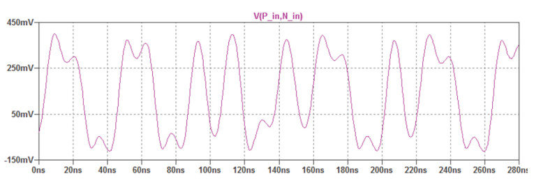
A port. Compare the general waveshapes to Figure 1.
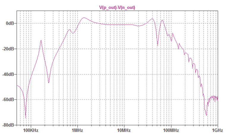
ADI’s A2B design guide offers layout advice for the A2B signals, which includes guidance that it should be treated as a controlled impedance differential design. While the design of the analog filter of Figure 3 limits the high-order harmonics it’s prudent to assume bandwidth extends out to at least the third harmonic of the 50MHz data, which with the Manchester coding spread would be up to 200MHz.
In FR-4 PCB material, 200MHz has a wavelength of 700mm, using the wavelength/10 rule of thumb for critical trace length, we find that traces less than 70mm shouldn’t be of concern. This is a long length relative to most A2B layouts. If we consider EMI, we might want to look out to a 500MHz bandwidth and that puts the critical length at 27 mm, which does fall in the range of many A2B designs. Though the distributed termination (i.e., the 120Ω resistors in Figure 3 and the 100Ω internal to the AD2428) raises the question of exactly what impedance the layout should target, ADI recommends 100Ω and without extensive alternate analysis 100Ω would be good advice.
Regardless of the length rules, as a differential signal, both the positive and negative differential signals should be matched in all aspects of components, layout, and routing to prevent common mode to differential mode noise conversion and to minimize EMI.
A2B Transceiver Device
Having worked through an agonizing amount of background material, we finally reach the point of looking at the actual chip that ADI sells to build A2B systems. Full details are in the datasheet so only a quick summary is offered here. Figure 6 summarizes the internal chip functions and outlines some of the connections. The resources available from the ADI website should be consulted for actual design details.
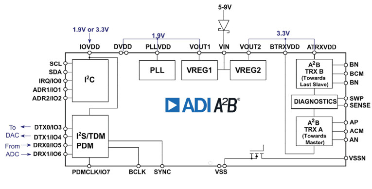
The chip operates across a wide voltage range, the low-end datasheet limit is 3.7V but to be able to supply phantom power, 5 V is a more practical lower limit. We’ve ignored the Schottky diode drop and for phantom powered slave nodes, VSS will not be 0V [5]. The chip includes two internal regulators, 3.3V for the LVDS section and 1.9V for the chip’s internal logic. The I/O section (I2S, I2C, GPIO) can be powered by 1.9V or 3.3V to match the voltage needs of peripherals. The regulators supply enough current to power the chip and provide about 25mA for a peripheral chip but a more rigorous computation is required for any actual system design.
The signals for the A2B bus (shown on the right side of Figure 6) were detailed in the second part of this article (November 2020). The CM pins each connect to a 4.7 µF to ground (along with smaller values to reduce ESR at high frequencies) and are part of the AC termination scheme inside the chip that uses two 100 Ω resistors, the other half to get to the required 50 Ω is provided by the network shown in Figure 3.
The I2C port can be an I2C slave when the chip is operated as an A2B master node or an I2C master when the chip is operated as an A2B slave node. In a slave node, it can also operate in I2C multimaster mode — simplifying the hardware design if the node requires a processor that needs to send/receive messages from the A2B host.
Like most chips, signal functions are multiplexed to try and support a large number of use cases without additional I/O expanders. GPIO lines can serve as interrupts back to the A2B host, as well as support a virtualized GPIO connection between the A2B master node and one or more slave nodes.
There are two sets of I2S data lines — one pair for input and the other for output. All support up to TDM32 mode with 16-bit or 32-bit word sizes. The input pair can also be used for PDM input. The AD2428 has dedicated bit clock and frame sync pins. For ADCs or DACs that need a master clock, the IO7 pin can be used. It also supplies PDM clock. ADI recommends 33 Ω series termination resistors on the I2S output pins, along with 27 pF to act as a low-pass filter to reduce EMI. This advice must be considered in the context of entire system design if the I2S or PDM connections are not point to point or traverse large impedance discontinuities (e.g., ribbon cables).
There is one specification on the AD2428 datasheet that will be of concern to anyone planning to use A2B for higher performance analog input and output: the unusually high I2S period jitter [6]. It ranges from typical values of 1.57 nsec RMS (one node hop) to 2.70 nsec RMS typical/5.5 nsec RMS maximum at the end of a 10-node chain. ADCs and DACs with good internal phase-locked loops (PLLs) will be able to handle some level of jitter, but determining the actual impact [7] is difficult as the jitter spectrum from the AD2428 is not defined by the datasheet. It’s also reasonable to assume the jitter has data and use case dependencies since the A2B bus is idle for different amounts of time based on the data slots used. A slave node’s PLL can only sync to the master when downstream data is going by.
To avoid extra design spins, high-performance audio applications should be prototyped and fully characterized to determine if the I2S jitter will need remediation. There are readily available ICs that can provide the needed clock functionality.
The AD2428 includes two “add jitter” features — one for the A2B bus and the other for the I2S interface — as a way to cheat on EMC testing by spreading the energy from periodic signals across a wider bandwidth. Use of this feature is not recommended in high-quality audio applications as: 1) the last thing any quality digital audio systems needs is more jitter; and 2) the total radiated energy is the same so it contributes to parasitic EMI pickup up in low-level analog circuits, regardless of how much jitter (bandwidth) spreading is used. Though the audible effect may be somewhat changed, it’s always best to not have the problem in the first place.
And In Real Life?
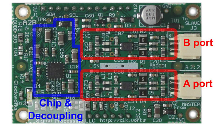
We’ll conclude the third part of this article with a look at an actual PCB to see how the various bits of theory, design rules, and circuits all come out in an actual product. Figure 7 shows one of Clockworks Signal Processing’s A2B modules with key sections highlighted. The module was designed to make A2B experimentation easy — all components are one side and no 0402 parts are used (mostly 0603 and 0805) so represents the upper bound for PCB real estate. A board with components on both sides and using smaller components with a compact layout can be done in half of the space. This module can act as a master or slave. A design that targets a specific mode of operation (along with the local or bus power choice) would need less parts.
Summary
In this article, we looked at the details of the electrical interfaces to the ADI AD242x chips. Guidance on the passive components needed for the interface was presented. In the final part of this article series, we’ll look at the tools and hardware available to create systems for development and evaluation. aX
Click here to read Part 1 of this article series
Click here to read Part 2 of this article series
Click here to read Part 4 of this article series
References
[1] “Low-voltage differential signaling,” Wikipedia
[2] H. Johnson and M. Graham, High-Speed Signal Propagation, Advanced Black Magic, Prentice Hall, 2003.
[3] AD241x, AD242x, Reference Schematics, Rev 2.1, Analog Devices, August 2019.
[4] Tech Note and LTSpice files, Clockworks Signal Processing
[5] B. LaMacchia, “Getting Started with Automotive Audio Bus (Part 2): Understanding A2B Features,” audioXpress, November 2020.
[6] J. Dunn, “Jitter Theory,” Audio Precision Tech Note TN-23, 2000.
[7] “Tech Note008 A2B I2S Clock Jitter,” Clockworks Signal Processing,
Sources
ADI’s main A2B web page provides links to part information, ADI tools, and design information, www.analog.com/en/applications/technology/a2b-audio-bus.html
This article was originally published in audioXpress, December 2020.