As explained in Part 1, unless your electronic device is fairly simple, a four-layer board makes sense because it offers dedicated ground and power planes in the middle, as well as a bottom layer for additional traces or power. This also avoids having to run both signal and power traces on the same layer that might complicate routing. Further, the inner layers avoid capacitive coupling between top and bottom traces that could, for example, cause a high-gain op-amp to oscillate if its input and output traces are opposite each other for much of a distance.
The top layer holds the component pads and most of the connecting traces, with the inner ground layer beneath. Then another inner layer carries power around the board, with the bottom layer available for any additional traces that can’t fit on top. To my thinking, laying out the routing of a PC board is somewhat like playing chess. You not only have to solve the current problem of how to connect component A to component B, you also have to think ahead several moves: If I put R35 here, will that block pin 6 of the op-amp from connecting to C12 over there? Would it help if I rotate the dual NOR gate 180 degrees?
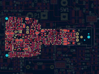
As Figure 8 shows, besides laying out the board traces, it’s just as important that the component labels (R12, C14 etc) on the silk screen layer clearly identify their related parts. Especially with tightly packed boards like my current project.
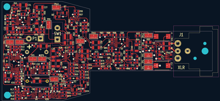
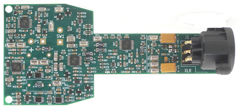
Photo 6 shows the completed board. I try to orient the text labels to align with their parts, but connecting lines were needed in a few places such as C33 near the middle of the board. The solid green-blue circles are holes through the board. The three large holes are used to align the board with the solder mask template when applying the solder paste, and also for later mounting in the case. The two small holes at right accept little nubs on the XLR connector to keep it aligned.
It’s fine for labels to cover traces, and even vias if needed, because those are coated with a clear protective film and don’t receive solder. Though avoid the holes in vias, or position letters such as “C” and “O” to circle the hole. KiCad uses short and long lines to identify ICs, with the longer line next to Pin 1. But I added small diamonds as text to mark Pin 1 even more clearly. I also added arrows to all the diodes to better identify their cathodes, and plus signs for the polarized capacitors to augment the too-small circles KiCad uses. Of course, a mass-produced board that’s assembled by machine doesn’t need these labels, so the parts layout could be even tighter.
That leaves the bottom layer shown in Figure 9 free for traces that need to cross traces on the top layer. Other than these few traces, the entire bottom surface is filled with copper. This circuit runs on a single 5V supply, so the bottom layer’s fill carries V/2 (2.5V) as a “center” pseudo-ground reference for the audio signals. Both KiCad and ExpressPCB create the fill clearance areas around traces automatically, though KiCad does a better job. With ExpressPCB you often need to draw a “keep-out” manually if the fill goes too close to a trace or via, or if a filled area ends up too narrow.
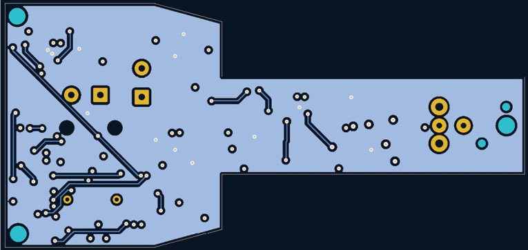
Also notice in Figure 9 that there are two types of vias that connect to traces on the top layer, shown as white circles. Vias without a black clearance around them connect this V/2 layer to circuit traces on the top. Vias with a clearance connect traces on top to one of the inner layers, or to traces on this bottom layer. Pads for leaded (through-hole) components or wires that connect to a copper fill can be either solid or “thermal relief” as shown in Figure 10. The pad is still connected to the copper fill, but having less copper makes it easier to manually solder the component leads quickly without the fill acting as a heatsink.

Fills are also used on the top layer when the layout isn’t as dense as this one. In that case the filled areas are connected to ground to minimize capacitive coupling between adjacent traces. It’s also possible to have SMD components and their pads on the bottom of the board. Though if you’re using solder paste and an oven, you might want to solder components on the bottom manually, after the top parts have been baked in place. I never tried using an oven a second time with the board upside down for parts on the bottom. But my friend Julia Truchsess insists that parts on top won’t fall off in the oven unless they’re large and heavy. The same surface tension mentioned earlier in Part 1 that slides the parts into alignment also holds them in place on the board when they’re upside down!
While we’re on the subject of soldering, it’s worth adding that solder flux is partially conductive. The standard DIY way to clean a PC board after the parts are soldered is to dip the board in isopropyl alcohol and clean it gently with a soft brush. Low impedance circuits can often get away without cleaning, and some types of solder paste (e.g., Chip Quik SMD291AX series) don’t require cleaning at all. Further, using solder paste with a template mask and oven doesn’t spread flux around the board as much as hand soldering does. But if you have any resistors in the megohm range it’s usually wise to clean the board.
Running Traces
Use appropriate trace widths and trace spacings based on the amount of current (width) and voltage (space) being carried. Of course, the board’s copper thickness is also a factor for how much current a trace can handle. With most modern solid-state circuits high voltage isn’t an issue, but manufacturing tolerances are. Many PCB manufacturers advise traces no narrower and no closer than 0.008”, though tighter tolerances might be available at a higher cost per board. If you stick with traces and spacing no smaller than 0.01” you’re guaranteed to be safe. This is another way KiCad is superior to ExpressPCB — KiCad won’t even let you put traces closer than the minimum specified in Preferences. Nor will it let you make an improper connection between components.
Never use 90-degree angles for traces. Sharp angles can end up narrower than the expected trace width when the copper is etched, and they are also more likely to peel off the board. It’s best to aim for 45 degrees, and here again KiCad is superior with an option to enforce that angle.
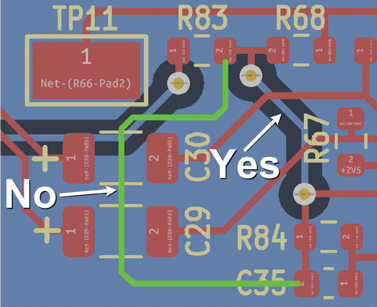
Short runs are always better than going around the block, even if that means using a via to get to the bottom layer. It might seem like cheating if you need to use a via, but electrically it’s better to keep runs short and close to the connected components. Figure 11 shows the top and bottom layers at the same time, with two ways to connect R83 to R84. Using a via is clearly preferred because it’s much shorter. Notice that the “No” trace passes between the terminals of C29 and C30. That by itself is fine, and there’s nothing wrong with routing a trace under most components between the pads if it fits.
ExpressPCB includes footprints for hundreds of standard parts, both through-hole and SMD, and KiCad includes more than 12,000 with more being contributed by users all the time. But it’s inevitable that you’ll eventually need to modify a part’s footprint, or design new footprints from scratch. Creating and editing footprints is easier in ExpressPCB than in KiCad, though many of the stock SMD outlines in ExpressPCB are slightly larger than needed. So when trying to pack as many parts as possible onto a small board, you’ll probably end up making some of them smaller.
Among its many View options, KiCad can show “courtyards” — the thin purple rectangles shown in Figure 8 surrounding each part. These display the physical size of the part as defined in its footprint. This lets you ensure that adjacent parts have enough clearance to avoid bumping into each other.
For solid-state devices having more than two pins, it’s important to verify that the pin numbers on your parts match the pin numbers on the board. Most transistors assign Pin 1 to the Base, Pin 2 to the Emitter, and Pin 3 to the Collector. But some are different. And some two-wire parts, such as Zener diodes, come in three-pin packages with one pin unused. The dual transistors I used in this project are available with two different pin-outs, so be sure you know which type you have!
It’s best to mount pots, switches, and connectors directly on the PC board to avoid hand wiring when possible. But sometimes these parts need to be on a separate panel. In that case you’ll add pads with through-holes to accept the connecting wires. Figure 8 shows two such pairs of pads for potentiometer P1 and switch SW1. Because these parts are in the audio signal path, I’m using shielded wire with the shield connected to the lower impedance. One is the output of an op-amp and the other is ground, with square pads identifying the shield connections.
ExpressPCB and KiCad both have plenty of standard pads with holes to choose from, but you need to choose pads with holes large enough for the wire’s gauge. Since most wires are stranded, you’ll probably tin the ends before pushing them through the pad holes. So figure the pad holes should be 15% to 20% larger than the wire diameter. There’s a terrific page on Wikipedia that lists the diameter for all of the standard wire gauges, plus other useful info, linked under Resources. Or better, measure a sample piece of wire yourself with a caliper after tinning it, as I do.
If you’re making a large number of very small PC boards, you might consider panelizing them into a larger group of connected “snap-apart” boards. If your board is, say, 1” by 2”, you could group six or 10 of them together with ¼” between. The board maker will saw partway through the board on each side, making it easy to snap them apart with your hands. Panelizing might make the boards easier for you to handle during assembly, or reduce the cost of each board. Just as important, if an outside shop does the assembly for you, they may require a certain minimum board size their automated machinery can handle. Many board makers can panelize boards for you. Just send them the files for one board, and they’ll figure out how to group and score them.
SMD Ceramic Capacitors
As a circuit designer, you already know how to choose appropriate capacitors for various functions. Common types are “can” and tantalum electrolytic for power supply filtering and audio coupling, ceramic for IC power supply bypass, and film when low distortion is needed for audio and other linear signals passing through the cap. My previous article, “Stop Worrying About Coupling Capacitors!” (audioXpress, May 2020) shows distortion amounts measured for a variety of capacitor types.
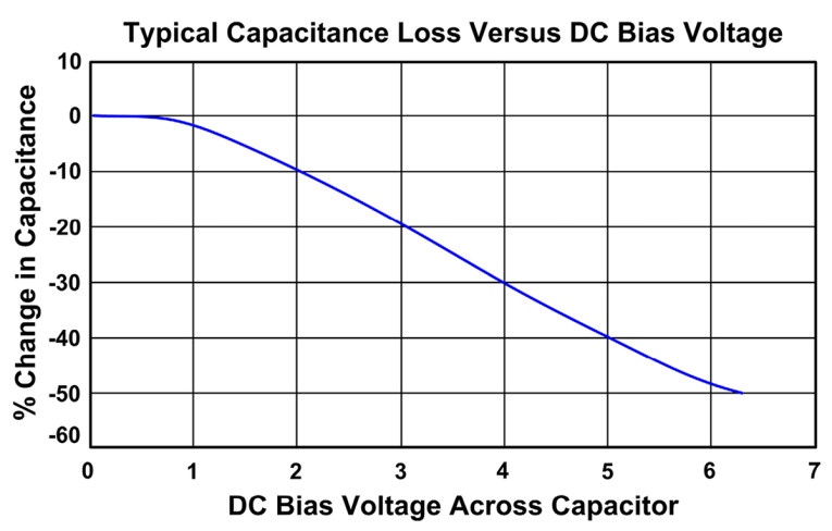
Ceramic caps are used for power supply bypass with ICs because they’re inexpensive, small, and their series inductance is very low. But there are several things to consider when choosing ceramic capacitors, especially the smallest SMD types. As mentioned in my earlier Null Tester article (audioXpress, June 2019), the value of some ceramic capacitor types is reduced dramatically as the DC voltage across them rises. This is due to their voltage coefficient. So a 10µF filter cap rated at 10V might indeed be 10µF with 1V DC across it, but only 5µF — half as much — when used to bypass a 6V power supply. Therefore, you often need to buy parts having more capacitance than required, based on the percentage reduction shown in the cap’s spec sheet under DC Bias Characteristics or similar wording. Class 2 ceramic capacitors (X5R, X7R) are pretty bad in this regard; Class 3 (Y5V, Z5U) are even worse, and their capacitance further varies with temperature.
An excellent article with more detail and explanations about ceramic capacitors is on the All About Circuits website (see Resources). Another helpful article is on the Murata website. Figure 12 shows the typical capacitance change for Class 2 and Class 3 capacitors versus DC bias voltage, derived from data on the Murata website. C0G and NP0 ceramic capacitors have a Class 1 dielectric, which is much better, and so are often good enough to send audio through when a film cap won’t fit. C0G/NP0 caps are larger than X5R and Y5V types, though not nearly as large as film caps having the same capacitance and maximum voltage ratings. A much more comprehensive explanation of ceramic capacitor properties and selection criteria can be found on Wikipedia (see Resources).
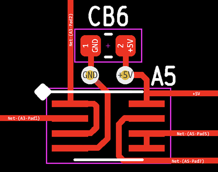
When laying out your PC board, you should place bypass caps as close as possible to their associated IC, with their traces and vias to the ground and power layers as short as you can manage. Figure 13 shows a close-up of a logic chip and its bypass cap CB6. The trace between A5 pin 4 and its ground via above is only 1/8th of an inch long, so it’s a lot closer than it looks! If this circuit needed to operate at much higher frequencies, it would not be wrong to add a second via to the ground plane right next to Pin 4.
The last step is to order the board, and optionally a solder mask template, from your chosen manufacturer. ExpressPCB is more expensive than ordering boards from China, even with international air shipping. But the software is not difficult to learn and use, and ordering is very easy right from within the PC board design program. You answer a few simple questions, click Get Price, and a few seconds later you know the final cost including shipping. So I gladly stuck with ExpressPCB until I needed ENIG gold plating, which it does not offer. My time and effort are worth more than the price difference between board makers.
KiCad is not tied to any particular vendor, so it outputs standard Gerber files that any manufacturer can use. However, it’s much more complicated to learn and use than ExpressPCB. If I had to start over with what I know now I would choose ExpressPCB again. But beware, the error checking in ExpressPCB is not as thorough as in KiCad. I designed my current board initially in ExpressPCB, and accidentally shorted the Ground and V/2 layers with vias rendering the board useless. KiCad automatically prevents such errors, so that could never happen.
Getting quotes and ordering boards from major companies can also be tricky. I found the AllPCB website to be rather confusing compared to ExpressPCB because there are so many options, such as copper thickness, board material, and choice of silk screen color. Of course, professional engineers will appreciate all those options! Thankfully, AllPCB has an online chat option where you can ask questions. Even easier, you can click a button to send them your files with a written description, and one of their salespeople will reply by email with a quote. aX
Resources
AllPCB | www.allpcb.com
“Ceramic Capacitor FAQs,” Murata, www.murata.com/en-us/support/faqs/capacitor/ceramiccapacitor/char/0005
ExpressPCB | www.expresspcb.com
KiCad | www.kicad.org
R. Keim, “X7R, X5R, C0G…: A Concise Guide to Ceramic Capacitor Types,” March 30, 2018, www.allaboutcircuits.com/technical-articles/x7r-x5r-c0g...-a-concise-guide-to-ceramic-capacitor-types
Wikipedia, “American wire gauge,” https://en.wikipedia.org/wiki/American_wire_gauge
Wikepedia, “Ceramic capacitors,” https://en.wikipedia.org/wiki/Ceramic_capacitor
E. Winer, “You Can DIY! Building a Null Tester Device,” audioXpress, June 2019,
E. Winer, “Stop Worrying About Coupling Capacitors!” audioXpress, May 2020,
Pragmatic Designs (Julia Truchsess) - www.pragmaticdesigns.com
This article was originally published in audioXpress, March 2023
Read Part 1 of this article - Modern PCB Design Practices: An Overview of the Process