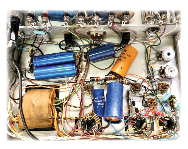
I learned to design and make PCBs in the 1970s while working for a high-tech firm. In those days we applied a special black paper tape, not unlike masking tape, to clear acetate to draw the circuit patterns. A piece of graph paper taped to the desk under the plastic helped keep the traces straight and orderly. This tape comes in various widths to make traces as wide or narrow as needed, though we taped the board layouts at double size for convenience and better accuracy. Round pads with holes for the electronic parts on the board using the same type of tape was available in various sizes. If you found an error or needed to move a group of traces, you had to lift the tape and pads, then do that section all over again.
Once the board layout was complete, the taped acetate went to a photo studio that created a negative at the correct size. We dipped blank copper-plated hard plastic boards into a bath of photo-resist liquid and hung them on edge to dry. Next, the photo negative was taped to a coated blank board, then exposed to ultraviolet light. Since this is a black negative image with clear slots where the traces will be, light passing through the slots cured those portions of photo-resist that would become the traces. The board was then dipped in acid to dissolve all the copper except where the traces were protected by the cured photo-resist. Finally, all the little pad holes for component leads had to be hand drilled in a miniature drill press.
When I resumed my interest in electronic design a few years ago, I used a pair of free programs from PCB maker ExpressPCB to draw schematics and lay out the boards. This software is very popular and extremely capable, though its internal file format is proprietary, requiring ExpressPCB to make the boards. I recently switched to KiCad, a newer free program that’s even more capable and also very popular. KiCad outputs standard Gerber files that can be used by any PCB vendor, such as AllPCB in China that I now use. That said, the tips and methods presented in this article are universal, and apply to any PC board layout software.
SMD Components
Old timers like me grew up using through-hole components and DIP integrated circuits, but many designs today use surface-mounted devices (SMDs). Instead of wire leads that go through holes to traces on the bottom of the board, SMD parts are soldered to flat pads on top of the board. Most SMD parts cost less than the larger older types, and many new parts are available only as SMDs, especially semiconductors. However, some through-hole parts may also be needed, such as large electrolytic power supply filter caps and mechanical pots and switches. But SMD trim pots are available and can be amazingly small, such as the Bournes TC33X series that are less than 4 mm (0.15”) in diameter. When possible, it’s best to put pots, switches, and connectors on the board to minimize hand wiring.
The first project I did using SMD components was the Null Tester featured in the June 2019 issue of audioXpress. I used mainly 0805 size parts because those are small enough to minimize the board size, but large enough to easily solder by hand. You can read about that in my Null Tester article linked under Resources. The size numbers for SMD parts are in 100ths of an inch, so 0805 means the part is 0.08” long by 0.05” wide. There are metric equivalents in 10th millimeters for each size, so 0805 is 2012 metric. For hand soldering, 0805 or larger is preferred, though it’s possible to solder 0603 parts by hand. Of course, you need fine tweezers, a soldering iron with a very small tip, and thin 0.025 or 0.020 solder. It also helps to have a lighted magnifier and a PC board vice to hold the board steady as you work.
My current project shown in this article has nearly 200 parts on a board that needs to fit inside a microphone case. So I used mainly 0603 resistors and capacitors, and similarly tiny sizes for the semiconductors. Photo 2 shows an assortment of the SMD parts I used, with an adjacent ruler to illustrate how incredibly small they really are. An 8-pin DIP IC is also shown for comparison. The 0603 capacitor, second from left and shown upside down, has “J” leads that wrap around under the part. This takes up even less room on the PC board, though having the pins under the part makes hand soldering much more difficult. Many other SMD parts are available with J leads. Even smaller part sizes are available when the boards will be assembled by machine. Resistors can be as small as 01005, and an 8-pin DSBGA IC is less than 2mm long!
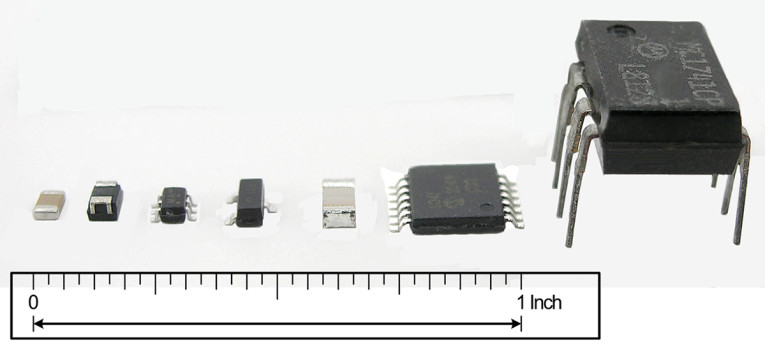
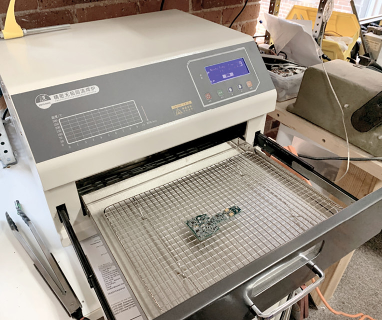
Photo 5 shows the oven used to flow the solder paste onto the boards (see Sources). Even if the parts are slightly misaligned on the board, surface tension causes them to slide into place when the paste liquefies in the oven. It’s a good idea to pay a little extra for gold plating—called Electroless Nickel Immersion Gold (ENIG)—on the component pads. When the solder paste is applied to the board through the template slots, you can more easily confirm that the pads are fully covered because the gold color changes to silver.
First Things First
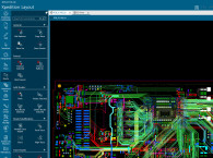
Before designing the PC board you need to draw the schematic in the PC board’s companion program. The Audio Input section of my schematic is shown in Figure 1. Both KiCad and ExpressPCB link the connections on your schematic to traces on the board. This not only confirms that your board matches the schematic, it can even guide you as you place the traces between parts by highlighting the destination pads. KiCad takes this further by letting you copy the schematic onto the board layout, then it shows a series of lines, called a “rats nest,” of all the board traces needed. As each trace is drawn and connected, that rats nest line disappears. If you remove a trace, the line re-appears so you can’t forget to connect it.
In KiCad, selecting a part in the schematic editor highlights the same part in the PCB program, and vice versa. This makes it easy to see where each part goes when you place them onto the board. Even better, if you use the optional plug-in to create an HTML Bill of Materials (BOM), it highlights all the parts having the same value. So when you select 100kΩ resistors, the board view shows all of them at once. You may need to flip two-wire parts around on the board layout so their orientation aligns with the schematic. Not only polarized parts like electrolytic capacitors and diodes, but resistors and non-polar capacitors also have a Pin 1 and Pin 2 that must connect correctly in order to match the schematic and avoid warning errors.
In ExpressPCB, you select a component’s physical size and shape — its footprint — when laying out the PC board. But in KiCad footprints are assigned in the schematic editor. This way, when you copy the schematic to the board, the correct footprint is already known and applied.
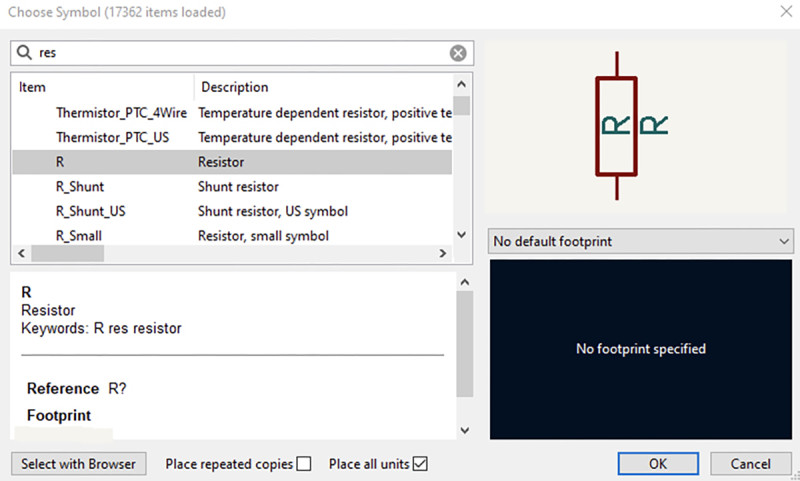
To insert a component into the schematic you select Add a Symbol, which brings up the Choose Symbol dialog shown in Figure 2. There are thousands of symbols from which to choose, so the Filter dialog at the top lets you pare that down by typing res (resistor) or opa (op-amp) or 74xx to show a list of all the known chips in that logic series. You can’t change the pre-defined library symbols, but you can copy, then modify, existing symbols, or create new symbols.
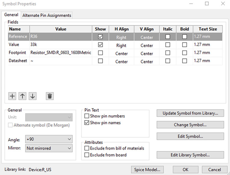
Next you double-click the symbol to bring up the Symbol Properties shown in Figure 3. This is where you assign the component’s number, value, and the footprint that defines the pad size and shape on the PC board. You can also include the URL for the part’s datasheet. That is then included when KiCad generates a BOM for your project, which is needed if your boards will be assembled by an outside company.
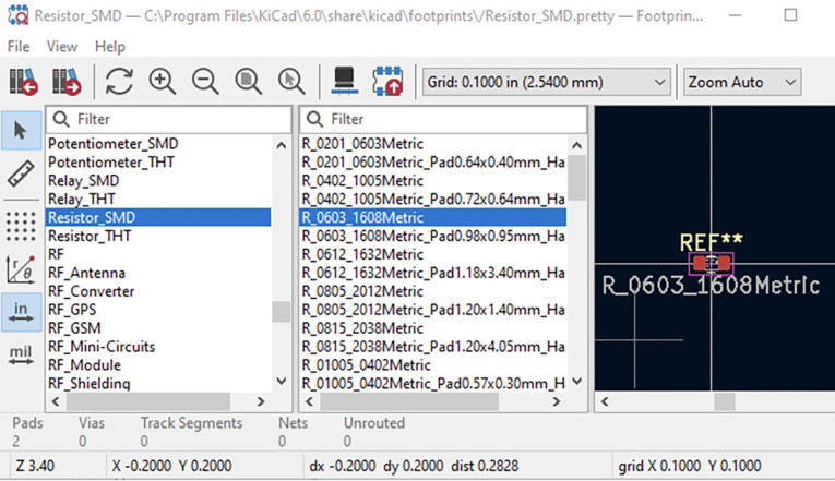
When you click the Footprint field, the dialog shown in Figure 4 is displayed, and an image of the footprint is also shown for confirmation. Most of the resistors in this project are 0603 (1608 Metric). After the first resistor or capacitor is added to the circuit and its footprint defined, you might find it easier to copy that part repeatedly rather than bother with Add Symbol each time. When you copy a component, its part number is replaced with a question mark (i.e., R?). Then when you double-click that part KiCad opens the Symbol Properties dialog for you to manually enter the new part number (e.g., R12).
Unless your device is fairly simple, a four-layer board makes sense because it offers ground and power planes in the middle. This eliminates capacitive coupling between the top and bottom signal traces, and helps to simplify routing. When you’re unable to route a particular trace on top because it would have to cross other traces, you’ll insert a via to pass that connection through to the bottom layer, then come back up on the other side. It also creates a sort of continuous bypass capacitor between the power and ground layers. The top layer usually holds most of the component pads and connecting traces, with the ground layer directly underneath. Then the power layer, with the fourth layer available for more connecting traces at the bottom and/or a second power source.
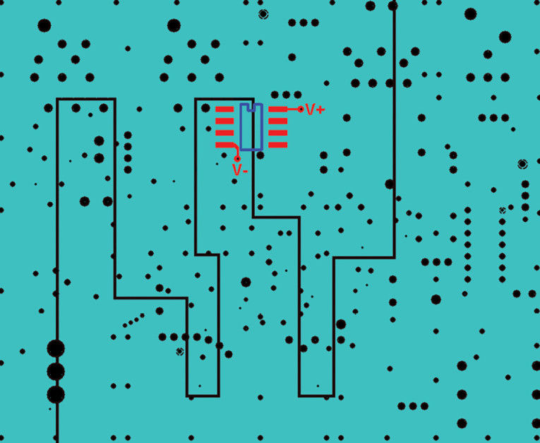
If many traces are needed on the bottom layer, and the circuit requires both plus and minus power, you can split the power layer to carry both V+ and V- as I did for my Null Tester board shown in Figure 5. As with most ICs, the plus and minus power pins for op-amps on the top layer are on opposite sides of the chip. I drew one “phantom” chip here as it would appear on the top, just to show how the chips can straddle gaps. Note that you don’t generally draw traces directly on the inner layers. But you can draw gaps, called “splits,” as shown here. Otherwise, you can use the power layer for V+ and the bottom layer for V- plus any additional traces needed.
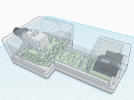
Note that PCBs don’t need to be rectangular. Most board manufacturers let you create round boards, or nearly any shape needed for your application. Mounting holes of any size can also be added to the board. Figure 6 shows the board for my current project, which is designed to fit inside a microphone case. All of the parts except one are on the top board layer and clearly identified as R12, C14, and so forth.
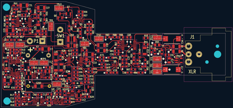
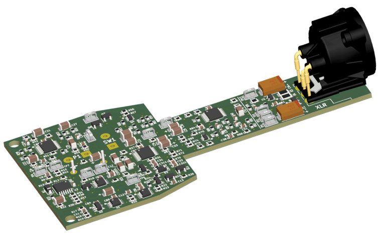
KiCad includes the 3D viewer shown in Figure 7 that lets you see a virtual photograph of the finished board. When using a separate CAD program to design an enclosure, this helps verify that the finished board will fit as intended. The pins sticking up from the bottom of the board near the middle left are for a 1” diameter dynamic loudspeaker used here as a microphone, mounted on the bottom. Notice the U-shaped test points scattered around the board—four are at the far right near two large capacitors and the XLR connector. These let you connect an oscilloscope or voltmeter probe to various parts of the circuit for troubleshooting. A final board design probably won’t need as many as used here.
Avoiding Errors
Both KiCad and ExpressPCB let you confirm that your board layout matches the schematic. Besides guiding you when connecting components, ExpressPCB lets you highlight related connections. With that tool selected, when you click on a component pad, all of the other pads that need to be connected are highlighted in blue. However, it doesn’t flag existing connections that are incorrect, or prevent you from connecting a via on top to more than one other layer. KiCad is much better in this regard. The schematic editor’s Electrical Rules Check provides warnings, such as parts that are not connected to anything, and also fatal errors, such as IC outputs that are connected together or to ground. KiCad’s PCB editor has its own error reporting module that displays warnings (e.g., silkscreen text items that overlap) and hard errors (e.g., short circuits between component pads or traces).
After a circuit is designed, I always buy all the parts before I even start the board layout. Then I can print the board layout in progress on paper to confirm that the part outlines and pads are in fact the correct size for what I received. Many SMD components are available in a bewildering number of minor variations, such as the time I received ICs much smaller than I thought I had ordered. Another time I accidentally bought a “wide” 1206 half-watt resistor that probably should have been listed as an 0612.
And Finally
Even if you need only one board, order at least two so you’ll have a blank board to examine and test without resistors and other parts blocking any labels or covering any traces. Some PCB manufacturers have minimums, such as five boards from AllPCB, which is the company that I use. But the cost for five boards is barely more than it is for one.
This article has presented an overview of the methods and procedures used to create modern PC boards. It also compared the features of two popular freeware programs for drawing schematics and laying out boards. Next month, Part 2 will go into greater detail, and present specific techniques to help you design PC boards that work correctly and are efficient.
Resources
AllPCB | www.allpcb.com
ExpressPCB | www.expresspcb.com
KiCad | www.kicad.org
Pragmatic Designs, Inc., Julia Truchsess’ website, https://pragmaticdesigns.com
E. Winer, “You Can DIY! Building a Null Tester Device,” audioXpress, June 2019,
Sources
Manual SMT Pick and Place Machine
Abacom Technologies | https://abacom-tech.com/product/manual-smt-pick-and-place-machine-ezpick
Benchtop Reflow Soldering Oven
AliExpress | www.aliexpress.com/item/2255799842971646.html
Pragmatic Designs (Julia Truchsess) - www.pragmaticdesigns.com
This article was originally published in audioXpress, February 2023
Read Part 2 of this article - Modern PCB Design Practices: Tips and Techniques