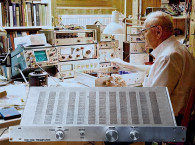
In Parts 1 and 2 of my JFET articles in Audio Electronics (see References with link for articles in PDF at the end of this text), I described the three basic circuits: common source, common drain, and the differential amplifiers. Using these circuits you can build up all low-level circuitry in phono preamps, line amps, crossovers, mike preamps, mixers, and so on. In fact, quite a few readers ordered small quantities of the JFETs for experiments. I had the impression that most of them wanted to make some simple crossover circuits, but a couple also experimented with mike preamps.
This simple amp has a gain of 33 times; i.e., 30dB. The frequency response is 300kHz! The distortion is dominated by second harmonics, which is to be expected from a square law device. At 1V RMS I measured 0.4% and at 3V RMS it increased to just over 1%. The linearity can be improved by increasing the supply voltage, as we have seen in Part 2.
This very simple amp would probably make many SE fans happy. Unfortunately, the circuit is not complete, in that the output is at a DC voltage of 12V, and requires a capacitor to isolate it from the next amp in the chain. However, capacitor coupling—whether in tube or in FET amps—always invites lots of discussion on the quality of the caps used (especially from those arm-chair amateurs who never build anything), so I always try to avoid them if possible!
Thanks to the availability of complementary devices in semiconductors (npn and pnp bipolars, and n-channel and p-channel FETs), it is easy to design DC-coupled circuits that do not use caps in the signal path. This article, therefore, focuses on DC-coupled amps.
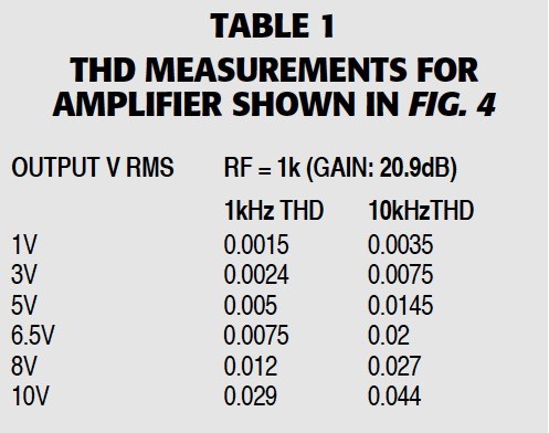
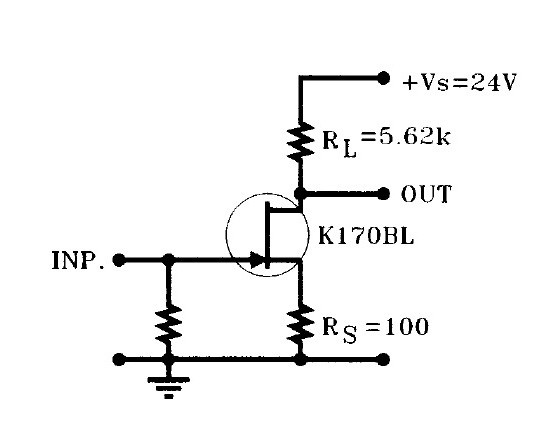
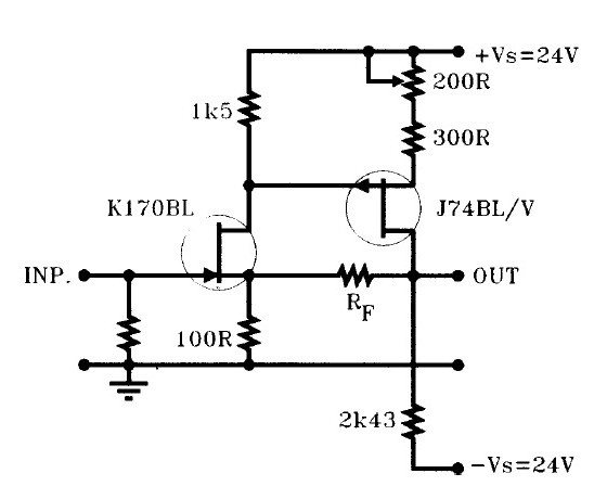
Figure 2 shows a two-stage JFET amp, in which the second stage, also a common-source amplifier, level-shifts the DC of the first stage to 0V. The drain voltage of JFET 1 is no longer required to sit at half of the supply voltage, because it is not responsible for the output voltage swing. The voltage drop across the drain resistor should, in fact, be as small as possible, to allow the second stage to work at maximum drain/source voltage.
I usually work with about 3V, which is a compromise between enough voltage to turn on the second-stage JFET, and enough to produce a reasonable gain. I selected 10mA drain current in the second stage. A small trimpot is inserted in the source circuit of the second stage, which allows trimming the output to 0V. The second-stage JFET must be selected for IDSS>10mA, to avoid operating it with positive bias.
The open-loop gain (the feedback resistor RF is open) is about 36dB and the frequency response is 150kHz. The reason for the relatively small increase of open-loop gain compared to the single stage one is that we have reduced the gain in the first stage by using a smaller drain resistor, and the second stage also operates with a small(ish) gain because of the small drain resistor and the local feedback in the source. THD has been reduced a bit for the same output level, because of the higher available voltage swing in the second stage: 1V = 0.3%, 3V = 0.93%. Maximum output voltage before clipping is >10V RMS.
I have indicated a feedback resistor RF from output to the source of the first stage. However, applying a useful feedback is not easy, since the source resistor, setting the operating point in the first stage, is fixed at 100R. If you want to have, say, a closed-loop gain of 10×, you would need an RF = 1k, which would load the second stage too much. Also, the open-loop gain of the amp is too low to have a useful amount of gain applied for feedback.
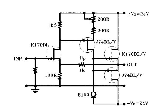
You can increase the open-loop gain, and thereby the available gain for feedback, by increasing the gain in the second stage. The easiest way to do this is to replace the 2k43 resistor (which supplies 10mA) with a 10mA constant-current source, such as the E-103 (Fig. 3).
The E-103 has a dynamic impedance of >100k and increases the open-loop gain by 20dB when the amp is loaded with a 10k resistor. Measurements show that this in itself does not improve the linearity of the stage, but now you have more gain that you can apply as feedback.
To address the load capability of the second stage, I have added a source follower to the amp (Fig. 4), described in Part 22 (Fig. 16B). The source follower adds a number of advantages to the amp: it isolates the feedback resistor from the high output impedance of the second stage, thereby further increasing the open-loop gain, and it provides a low output impedance to drive the feedback resistor and outside load.
Closed-loop gain with RF = 1k is 20.9dB. The closed-loop frequency response is more than 1MHz! Table 1 shows the THD measured on this amp. Overall a simple, but very good, SE line amp!
The Complementary Game
Although this SE amp functions well, I have two issues with it. The first is its DC stability. As described in Part 11, the transconductance curve of JFETs is temperature-dependent, and unless you operate it at zero tempco, you will have a temperature drift. Of course, a few mV of drift is acceptable in most audio applications; however, here we will try to minimize this as much as possible. Naturally, the open-loop linearity can also be improved. Enter the fully complementary circuitry.
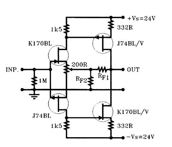
Consider the circuit in Fig. 3 as half of such a complementary circuit. Imagine folding down this circuit along the horizontal ground line, naturally replacing the n-channel with p and vice versa. Figure 5 shows this basic 4-JFET configuration. The trimpot is used to adjust the output offset to 0V.
I have kept the same currents in both input stage and second stage at 2mA and 10mA as before. Since the second stage consists of two JFETs connected together at their drains, they act as constant-current sources to each other. The amp therefore becomes a transconductance amplifier, converting input voltage to output current. The conversion back to voltage happens when you connect a resistor from the output to ground as a load resistor, or back to the negative input as a feedback resistor.
Here a feedback resistor is shown, representing the load at the output. The open-loop voltage gain is therefore very much dependent on this load resistor. I am usually using RF1 = 2k21 feedback resistor; open-loop gain is equal to 42dB with this load. The open-loop frequency response is about 150kHz, same as the SE circuit.
Open-loop distortion is almost an order of magnitude less than for the SE circuit, indicating that the complementary circuit, depending on the matching of the JFETs used, is cancelling some of the second harmonic distortion. DC stability has also improved significantly due to the use of complementary devices cancelling the drift.
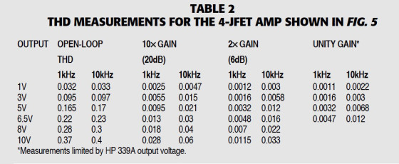
There are many more possibilities in terms of applying feedback than with the SE circuit, and you can produce a number of useful circuits. If you select RF1 = 2k21 and RF2 = 221R, you will have a line amp with 20.9dB gain. You can also make RF2 = 2k21 for a 6dB amp, which is very useful as a buffer between your CD player and your power amp, when you need a volume control in-between. If you remove RF2 completely, you will have a unity gain buffer. Table 2 shows the THD for this buffer with different gain settings.
Reducing The Input Capacitance by Cascoding
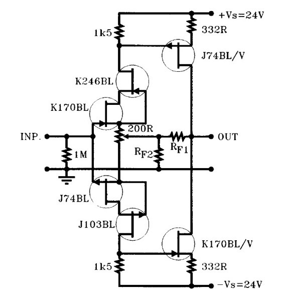
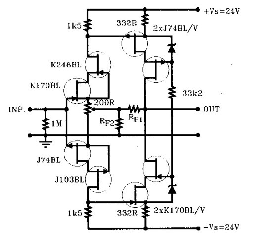
The input capacitance of the basic 4-JFET circuit in Fig. 5 is about 28pF. This is normally no problem when the source impedance is lower than 10k. However, the input capacitance of the JFETs is voltage dependent, and when driven from high impedance it might cause distortion. You might recall that we solved this problem in Part 1 by cascoding the input JFET with another one (Fig. 9A/B in Part 1). This circuit is shown in Fig. 6. The cascoding reduces the input capacitance to less than 2pF, and there is no sign of any distortion with high source impedances.
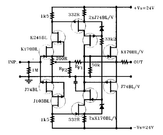
Cascoding the second stage as well (Fig. 7) can make further improvements. This helps reduce the internal capacitances and capacitance modulation. However, all these circuits have a high output impedance and because the open-loop gain is limited, even the feedback cannot reduce it to very low levels.
Of course, this is not an important factor in normal line amp applications; however, when used as a unity gain buffer in filter applications, it is essential. I have therefore added a complementary source follower to the output. Figure 8 shows the final all-JFET “Super Buffer.”
Since there is no load on the second stage, the open-loop gain is very high. In fact, it is too high for my liking, and I usually reduce it with a resistive load on the second stage. With 50k the open-loop gain is 67dB. Open-loop frequency response is close to 20kHz.
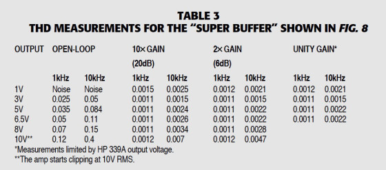
The THD for four different gain settings is shown in Table 3. Note the very low open-loop distortion indicating very good linearity. Due to the voltage drop across the bias circuit in the second stage cascode, the amp starts to clip just around 10V RMS. This is responsible for the slightly increasing THD levels at 10V. A higher supply voltage would allow more output without clipping.
The amp needs a series resistor at the output (47Ω) for stability. The actual output impedance of the amp is about 2Ω, and with the series resistor it’s 50Ω. The amp can drive loads down to 1kΩ, with no increase in THD. The frequency response with 10× gain is more than 1MHz! In unity gain it has a rise time of <100ns, indicating a frequency response well into the MHz region.
The circuit also shows very good noise performance. Measured in the 10× gain position with 2k21/221R feedback resistors, the input noise is <0.4μV over the audio bandwidth. You can further reduce the input noise by paralleling several input stages.
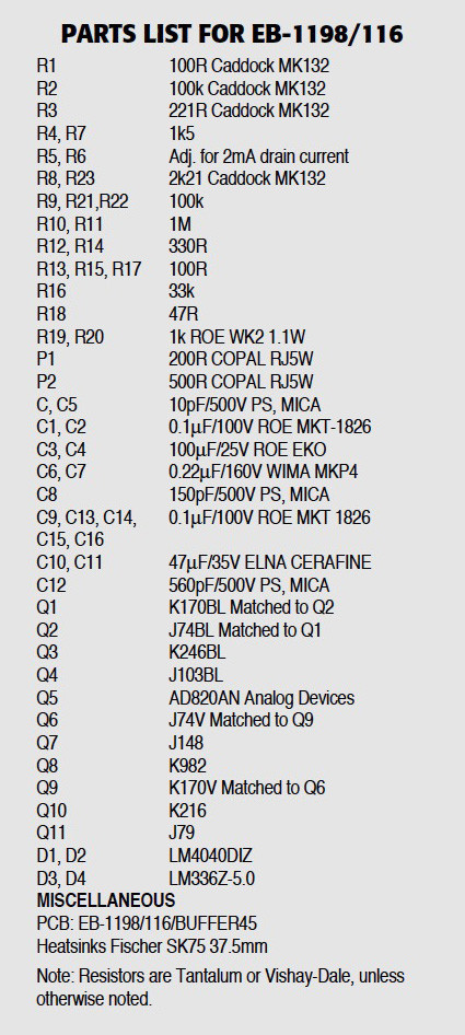
The All-FET Line Amp (EB-1198/116)
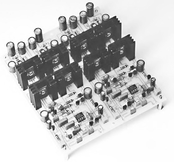
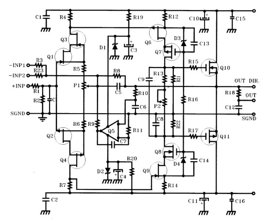
I have used the amp shown in Fig. 8 in many line amp and filter applications with very good results. It’s simple, inexpensive, and has an extremely high resolution. However, for a commercial product I wanted even higher drive capability. My goal was to be able to drive loads down to about 100Ω in pure Class-A, also allowing it to be used as a headphone amp. To be able to drive 100Ω in Class-A with up to 10V RMS, you need to have a bias current of 70mA. There are no JFETs that can withstand this power dissipation, and I used MOSFETs as output devices. The schematic of the all-FET line amp is shown in Fig. 9.
The input JFET-cascode, consisting of Q1-Q2-Q3 and Q4, is operated at 2mA, and Q1 and Q2 must be matched to ±10% of IDSS. Q1 and Q2 are selected from the “BL” group, and, depending on IDSS, they are adjusted for ID = 2mA by R5 and R6. (For selection of JFETs see the test jig described in Part 1.) Q3 and Q4 must have a gate-source voltage of minimum 2V at this current, to provide proper drain-source voltage to Q1–Q2.
The second stage, consisting of JFETs Q6–Q9 and MOSFETs Q7–Q8, operates at just below 10mA. Select Q6 and Q9, which must be matched to each other, for IDSS>10mA. It is easiest to select these from the “V” group, because the minimum IDSS for this group is 10mA (IDSS: 10–20mA). I am using MOSFETs as cascode devices because I wanted to try the circuit with higher supply voltages than the JFETs would allow. The output devices, Q10–Q11 (Hitachi TO-220 MOSFETs), are operating at approximately 70mA; proper heatsinking is therefore mandatory.
Although the DC stability of the amp is very good, I added a servo to ensure very low offset voltage, independent of the ambient temperature. Q5 is a JFET input servo amplifier, providing tracking of the output offset to less than a couple of mV. The RC networks of R10-C6 and R11-C7 filter out all AC signals over 1Hz. The servo is therefore only operational under 1Hz, and should not affect the sound of the amplifier. Nevertheless, if you believe that it does, don’t hesitate to try different op amps for this. D1 and D2 are IC shunt regulators, supplying Q5 with ±10V.
For an all-out line amp, the best resistors are the Vishay S102s and the Caddock MK132s. Personally, I prefer the Caddocks, which seem to be more neutral than the Vishays. However, you don’t need to use all-Vishays or all-Caddocks to get super sound; only the input and feedback resistors (R1, R2, R3, R4, R7, and R8) should be from these. The rest could be Tantalum (I have found these give the best combination with the Caddocks), but DALE RN60s are also good (but only the ones using non-magnetic construction). The frequency compensating capacitors are polystyrene or Mica caps, the electrolytics C10 and C11 are ELNA CERAFINE, and the rest of the caps are WIMA and Roederstein.
The open-loop gain of the amplifier is kept at a relatively low 66dB by the two resistors R21–R22. Open-loop frequency response is 20kHz (−3dB)! Open-loop THD is very low: 0.055% at 1kHz, 3V RMS and 0.095% at 10kHz, 3V RMS. This is reduced to below the measurement limit of the HP 339A distortion analyzer when feedback is applied with resistors R8–R3.
Normally, R8 is 2k and R3 is 221Ω. This gives a closed-loop gain of 20dB. Changing the ratio of R8–R3 can reduce the closed-loop gain. The rise time of the amplifier is less than 200ns for an output of +10V. Closed-loop frequency response is over 1MHz! Output impedance is less than 10Ω at the “direct” output and is approximately equal to R18 at the “normal” output.
The all-FET line amp also has lownoise, wideband regulators on the PCB (schematic not shown here). These are using low-noise JFET-input op amp and MOSFET outputs. The power-supply requirement is ±29V unregulated voltage at 100mA per channel. A high-quality power supply with fast/soft recovery diodes and high-quality 10,000–22,000μF electrolytics is recommended.
Two of the line amps can also be connected for balanced operation.
Testimonials
Finally, here are a couple examples of authentic customer feedback from the US and Canada:
“After living with the line amp for quite a few weeks now, I would say the following is what I hear:
• incredible resolution in loud, congested orchestral passages; e.g., locating triangles on top of full orchestra
• amazing sense of “air,” space, width, depth; i.e., imaging is holographic
• startling resolution in what I call “leading edge transients” on, for example, brass, drums, and so forth.
I could go on and on, but, you’ll think I’m hyperbolizing! I can’t imagine improving on your design.”
“It (the all-FET line amp) has extraordinary detail, very accurate harmonic structure, powerful macro and micro dynamics, and an extremely low noise floor allowing effortless transient attack, and vocal intonation and ambient decay to be vividly portrayed…”
Acknowledgment
Many thanks to Walt Jung of Analog Devices for his valuable comments and suggestions.
References
1. Erno Borbely, “JFETS: The New Frontier, Part 1,” Audio Electronics 5/99.
2. Erno Borbely, “JFETS: The New Frontier, Part 2,” Audio Electronics 6/99.
Download both articles in PDF here
This article was published in audioXpress, May 2002.