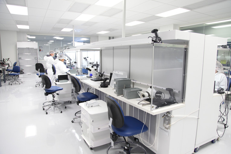
Sensor elements and other critical assemblies are manufactured within a 1,200 sq. ft. room, which meets or exceeds ISO Class 7 cleanliness standard (less than 10,000 particles per cubic foot). This room is also humidity controlled within a tight specification. Particle counts are further reduced down to ISO Class 3-4 levels (less than 10 particles / cubic foot) due to usage of laminar flow benches, High Efficiency Particulate Air (HEPA) filtered fume extractors and other state of the art clean room equipment.
A second clean room area (3,100 sq. ft.) is designated for final product assembly and calibration processes. This space is under even stricter humidity controls to prevent electrostatic discharge (ESD) damage to electrical components. Laminar flow benches for critical product assembly, and solder stations with HEPA filtered fume extractors are used throughout this space.
PCB expects that the environmentally controlled clean rooms will further enhance their pressure and force sensor manufacturing and assembly processes. Higher efficiencies, increased throughput, and improved quality and delivery are just some of the expected benefits. PCB design engineers are already working on the next generation of high performance sensors, whose design and manufacturing is dependent upon a clean room environment.
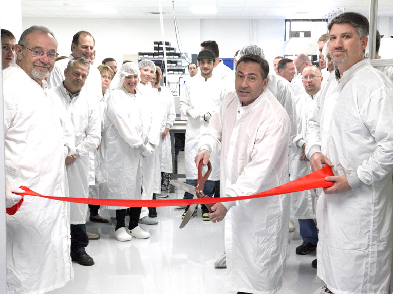
“We are very proud of this new state-of-the-art facility and our continuous improvement initiatives to provide higher performing, quality sensor products to meet the demands of our valued customers,” says David T. Hore, President of PCB Piezotronics. “This large investment in a world-class manufacturing environment reinforces PCB’s commitment to Total Customer Satisfaction, which is our company’s long-standing mission.”
PCB Piezotronics is a designer and manufacturer of microphones, vibration, pressure, force, torque, load, and strain sensors, as well as the pioneer of ICP technology used by design engineers and predictive maintenance professionals worldwide for test, measurement, monitoring, and control requirements in multiple industries.
www.pcb.com