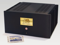


The completed PhL-100 device is shown in Photo 1. To begin, all the amplification stages in my PhL-100 design are based on top-quality audio op-amps from Texas Instruments (TI), where I selected the OPA1642 for the phono stage and OPA1612 for the line/headphone stage. Almost all the components of the device are contained on a single PCB for easy construction.
Figure 1 shows the simplified block diagram of the PhL-100 device with all the parts of the preamplifier—the MM phono stage, the line and headphone amplifier, the protection circuit with the indication LEDs, and the power supply.


The Phono Preamplifier Circuit
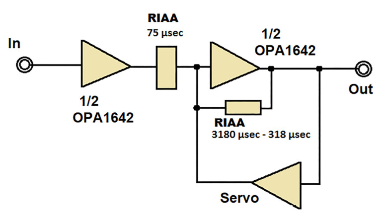
The detailed block diagram of Figure 2 shows that each channel consists of two gain stages and a DC servo circuit that eliminates the output offset. The first stage buffers the cartridge and provides a gain of 21.3dB. A passive circuit follows with the RIAA equalization time constant at 75μsec. The second stage provides additional gain and the 318μsec and the 3180μsec time constants of the RIAA curve.
The electronic schematic is shown in Figure 3. A detailed description of the operation follows, which refers only to the Right channel, since the other is identical. Resistor R2 and capacitor C5 adjust the load for the moving magnet (MM) cartridge. Both should have the recommended values by the cartridge manufacturer. The schematic shows the typical values of 47kΩ and 100pF.
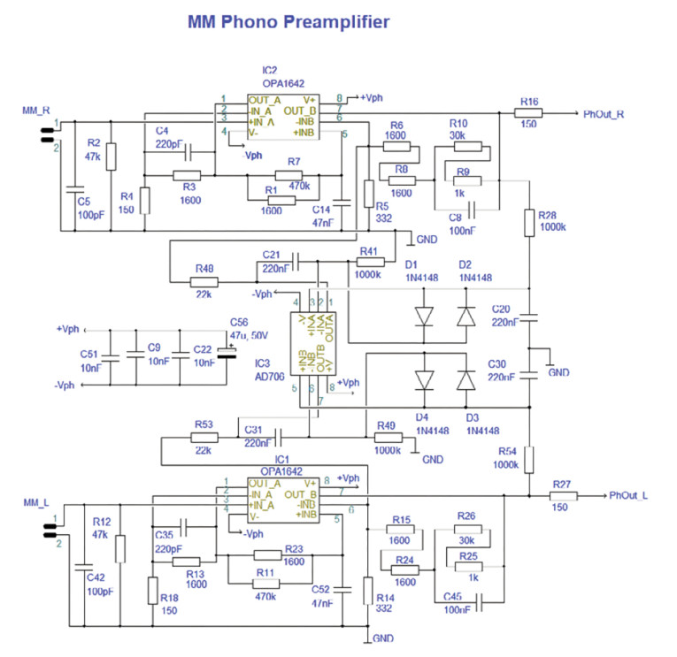
The first stage is a non-inverting amplifier based on an OPA1642. This is a JFET-input, ultra-low distortion, low-noise, dual op-amp fully specified for audio applications. The gain is 21.3dB and it is defined by resistors R3 and R4, which have low values for minimum noise. This gain is suitable for cartridges with a nominal output about 5mV @ 1kHz, 5cm/sec. If the cartridge has a different nominal output, the gain should be adjusted accordingly by changing the value of R4. The capacitor C4 with R3 give a high frequencies roll-off at about 300kHz.
Resistors R1, R7 and capacitor C14 form the time constant of the RIAA equalization at 75μsec (2122Hz). I used high accuracy resistors with 0.1% tolerance and polypropylene capacitor with a tolerance of 2% to minimize the deviations of the circuit from the RIAA curve.
The next op-amp stage is based again on the OPA1642 op-amp and forms the time constants of the RIAA equalization at 3180μsec and 318μsec with the resistors R5, R6, R8, R9, R10 and the capacitor C8. Here again I used high-accuracy components.
The total gain of the phono preamplifier is 42dB at 1kHz. Resistor R16 buffers the output of the phono stage before it is connected to the Line preamplifier.
The circuit around IC3 is a non inverting DC servo integrator, which keeps the output of the RIAA preamplifier very close to 0VDC. The use of the servo circuit eliminates the use of a capacitor in the feedback loop of the amplifier. The Analog Device AD706J is used for IC3, which is a dual, low power, bipolar op-amp with 100μV input offset, and input bias current < 100pA with low drift over temperature. The output voltage of IC3 through resistor R48 adjusts the voltage of the inverting input of the second amplification stage in order to eliminate any DC offsets at the output.
The Line/Headphone Amplifier Circuit
The electronic schematic of the line and headphone amplifier is shown in Figure 4. The selection of the input signal of the preamplifier is performed by two high-quality relays per channel, K1 and K2 from Panasonic, type TXS2-12V-1 with AgPd contacts, suitable for use in low level load analog circuits. Across each relay coil, protection diodes are used (D16-D17). Each external input has one dedicated double pole relay that connects or disconnects completely both the positive and the negative part of the signal from the preamplifier circuitry.

Resistor R17 or R29 with capacitor C3 form a low-pass filter at about 230kHz, (assuming that the previous stage’s output impedance is not greater than 200Ω) to attenuate any electromagnetic interference (EMI) that could enter to the circuit. Next, there is the connector for the volume control potentiometer, which is placed on the device’s front panel. The volume control’s position at the input protects the preamplifier from any possible overload that could caused by high level input signals. I used a rotary stereo logarithmic potentiometer from Alps (type RK27112-LOG50k). The capacitor C11 is included for the DC protection of the line amplifier circuitry and it is the only capacitor used in the audio signal path. Resistor R33 needs to ensure a DC path for the op-amp proper operation.
The amplification stage is built around IC5A, which is an OPA1612 connected as a non-inverting op-amp circuit. The OPA1612 is a bipolar, ultra-low noise (1.1nV/√Hz at 1kHz) op-amp with an ultra-low distortion (0.000015% at 1kHz). It offers a rail-to-rail output swing with a high slew rate of 27V/μs at 2kΩ load, which increases headroom and maximizes dynamic range. It is also unity gain stable and has a high output drive capability.
The gain defined by resistors R51 and R55 is set at x8 (18.1dB). Resistor R55 has a low value for minimum noise contribution to the circuit. The value of capacitor C12 was selected so that the roll-off of the high-frequency response will be at about 320kHz.
Resistor R43 buffers the output of the IC5A from the next stages that consist of five OPA1612 op-amps (IC5B, IC6A, IC6B, IC7A, and IC7B) operating as voltage followers with their outputs connected in parallel by 10Ω resistors. The total maximum output current capability as
I measured is about 200mArms. The components R45 and C54 at the output help keep the high-frequency stability when driving long cables or difficult loads.
Resistor R90 buffers the output of the line preamplifier from capacitive loads in case long cables are connected from the preamplifier to the power amplifier.
The outputs are isolated from the circuit through relays, which close with a short delay during the power up and disconnect very quickly during power down. Also they can be disconnected manually when the MUTE switch is energized. The circuit around IC4 is a DC servo integrator similar to the one used in the phono stage to keep the output of the amplifier very close to 0VDC.
The Power Supply Circuit
The PhL-100 needs an external regulated power supply between ±12.6VDC to ±15VDC, with a minimum current capability of ±0.5 A. It could operate with lower voltages if the Zener diode Z2 of the protection circuit is changed to a lower voltage.
I used a low noise external power supply based on capacitor multipliers and LM317 to LM337 voltage regulators, similar to the one I used for my headphone amplifier published in audioXpress, June 2013 (see Resources). The voltage outputs of this power supply were ±12.6VDC.
I also used an external desk-top switching power supply for the PhL-100. It has a ±15VDC output with 5% total regulation and a minimum switching frequency at 24kHz, which is outside of the audio bandwidth. With both power supplies the PhL-100 operated very well without any noticeable difference.
Through a 5-pin DIN connector on the back panel of the PhL-100, the voltage goes to the power connector on the PCB. The schematic of the power supply circuit is shown in Figure 5.
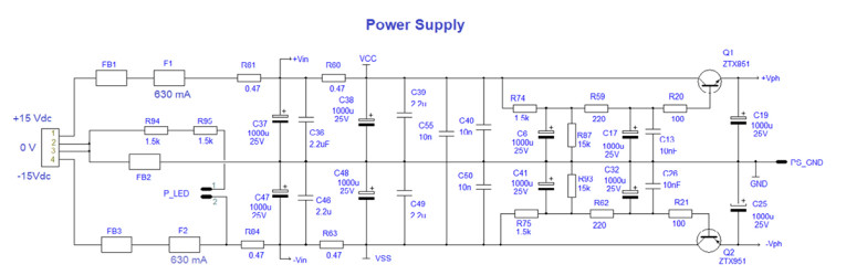
Fuses F1 and F2 are slow-blow fuses, mounted on the PCB to protect the external power supply from short circuits within the device. FB1, FB2, and FB3 are ferrite beads inductors offering electromagnetic induction (EMI) protection from several megahertz up to gigahertz by suppressing any noise coming from the power supply. Resistors R60, R61, R63, R84 with capacitors C37, C38, C47, C48 form low-pass filters to eliminate any possible noise from the power supply.
The phono circuit is supplied through a capacitor multiplier circuit to further eliminate the noise. Transistors Q1 and Q2 are low noise types and form the capacitor multiplier for the positive side and the negative side, respectively. Resistor R87 and R93 are used to set a 2VDC voltage drop between the collector and the emitter of Q1 and Q2 for proper operation of the circuit.
The Protection Circuit
The schematic of the protection circuit is shown in Figure 6. The circuit supports the following functions: When the preamplifier is powered on, it connects the output through a relay after a short delay to avoid any transient noise to the following equipment. It quickly disconnects the output relay when the preamplifier is powered off or when a sudden power loss happens.
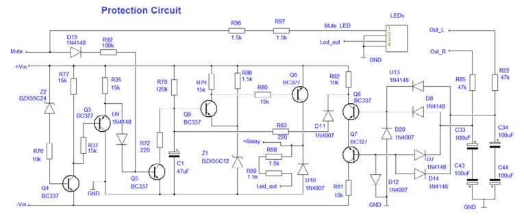
Using the MUTE switch, the output can be manually disconnected. The circuit also protects against a malfunction that could produce high DC voltage at the output of the amplifier, protecting the expensive headphones.
When the power is applied to the circuit, the components Z2, R76, and Q4 detect the presence of the DC voltage and when this voltage goes higher than about 25VDC, the transistor Q4 is set to the On state. This also activates transistor Q3 which short circuit the diode D9 to the ground deactivating the transistor Q5.
The Zener diode Z1 generates a 12VDC constant voltage, which is used for the output relay’s activation in conjunction with the capacitor C1’s voltage, which is increased slowly by R78. When it reaches about 12.6VDC, the transistor Q9 is activated and turns on the transistor Q6, which turns on the relay K5. The LEDout is connected in parallel with the output relay through the current limited resistors R98 and R99. When the LED illuminates, it indicates that the output is normally connected.
D15 with R92 are used to activate transistor Q5 with an external voltage coming from the manual MUTE switch. In this case, Q5 is turned on and deactivates the relay K5 through transistors Q9 and Q6.
Any large DC offset at the output is sensed by the circuit around transistor Q7 and Q8 with diodes D7, D8, D12, D13, D14, and D20. The components R22, C34, and C44 for the Left Channel and R85, C33, and C43 for the Right Channel create a low-pass filter at a very low frequency to avoid activation of the protection circuit by strong bass frequencies of the output signal.
The Construction of the PhL-100
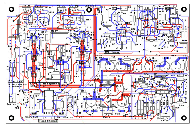
I used the Design Spark PCB software to design the PCB. The outcome was a 200mm × 130mm double-sided PCB with ground planes on the top and bottom layers. One PCB is used for both Left and Right channels.
Figure 7 shows the PCB’s complete guide assembly. The Parts List shows what is required to build the preamplifier. I used high-quality parts for the preamplifier’s construction like 0.1% resistors and polypropylene capacitors where needed.
For the assembly of the PCB, I started by placing and soldering all the components of the Power Supply section. I connected the power to the circuit and I checked that the voltages at pin 8 and pin 4 of all the op-amps of the Line and Headphone amplifier were about 0.1VDC less than the input voltage. The voltages at the op-amps pins of the Phono section should be about 2VDC less. I did this to be sure that all the SMD op-amps will find the correct voltage when they will be soldered on the PCB. This eliminates the risk to destroy the expensive op-amps if something goes wrong with the power supply.
Then I removed the power and I soldered all the SMD op-amps (8-lead plastic SOT-23 package) with my standard soldering iron using a very thin tip and a 0.38mm solder wire. A desktop magnifier with a LED light helped me do the job correctly. The assembly of the other through-hole components is very easy and it should be done from the smaller to the larger components.
Resistors R22 and R85 should not be soldered to the PCB as they will be used later to check the protection circuit. I used a metal enclosure with an aluminum front panel to house the components of the preamplifier. The enclosure had the following external dimensions: Width= 270mm, Depth=200mm, and Height=45mm.
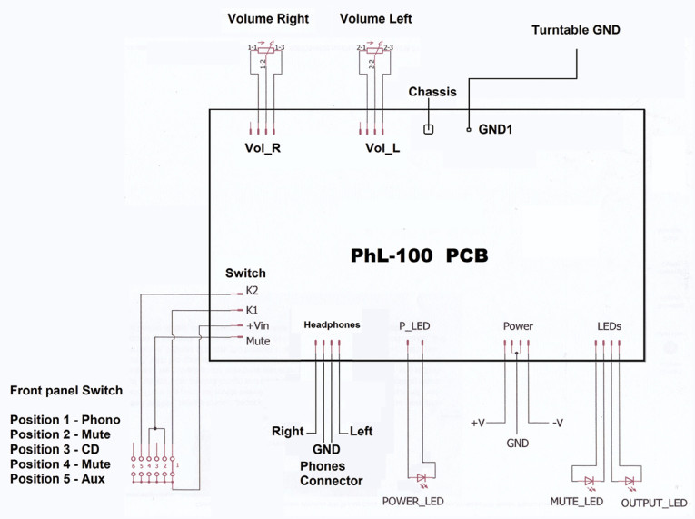
Figure 8 shows the internal wiring of the PhL-100. To eliminate any possible noise at the output when switching between the three inputs, I inserted two extra MUTE positions between them. For example, to switch from CD to the AUX input, the switch goes first to the MUTE position which disconnects the output and then to the AUX position where the output is connected again with a delay.
On the left side of the PhL-100’s front panel (Photo 1), the red LED indicates the operation and the green LED indicates that the output is connected. Next, there is the Input Selection switch and in the middle is the headphone connector. Between them, one 3mm red LED indicates that the muting circuit is active. I placed the volume potentiometer on the right side of the panel.
The text on the front plate was created using the “Front Panel Designer” program (see Resources). The file was printed on a transparent self-adhesive sheet with my ink-jet printer.
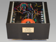
The back panel of the preamplifier is shown in Photo 2. On the right side, there is a 5-pin DIN connector for the supply of the preamplifier. On the left side, there are eight gold-plated RCA female connectors for the inputs and the outputs of the preamplifier. They are placed with the same order as that of the PCB giving a very neat internal wiring as shown in Photo 3.


Testing the PhL-100
After the construction was complete, I checked all the power supply voltages for both channels. I checked also that the servo circuits were operating within their limits. This means that the voltage at pins 1 and 7 of IC3 and IC4 should be between -2.5VDC to +2.5VDC or so. In my prototype, the voltage ranged from -0.3VDC to -1.5VDC.
The protection circuit should be tested and ensured that it operates correctly when a DC fault appears at the output. As I mentioned, R22 and R85 were not soldered on the PCB. To do the testing, the pins of R22 and R85 that are close to the K5 relay are left free and the other pins are soldered to the PCB. This is necessary because an external voltage will be connected to the free pins and I didn’t want to put the outputs of the op-amp’s IC6, IC7, IC9, and IC10 at risk.
I connected an external positive voltage of +3VDC directly to the free pin of R22 with the ground of the +3VDC connected to the ground of the PhL-100. This should deactivate the output relay disconnecting the output. I repeat the same with a negative voltage of -3VDC.
The same procedure is performed for the other channel, with the external voltage now connected to the free pin of R85. After the successful completion of the test, the free pins of R22 and R85 are soldered to the PCB.
One final thing to notice is that both preamplifier and headphones outputs are active simultaneously. This could be inconvenient if someone wants to only listen with the headphones. I don’t have that problem since I can mute the DSP digital crossover with my system.
One solution can be a high-quality switch that would disconnect the preamplifier’s line output signal. Another option would be a switched headphone connector (e.g., the Neutrik NYS216G), which would switch off the line out when the headphones are connected.
Measurements of the PhL-100
I measured the accuracy of the preamplifier’s RIAA curve with an accurate inverse RIAA network, which was constructed with high-accuracy components. For more details about this network see my article “The MC100 A High-Quality Moving Coil RIAA Preamplifier” (audioXpress, March 2014) Figure 9 shows the preamplifier’s accuracy with this inverse RIAA network connected at its input. The deviation from the ideal RIAA curve is about ±0.1dB from 20Hz to 10kHz. Of course, this includes the error of the inverse RIAA network and the preamplifier.

The input impedance of the line preamplifier at 1kHz ranges from 30kΩ to 50kΩ, depending on the position of the Volume potentiometer. The maximum gain of the line preamplifier is 21.6dB. The -3dB points of the frequency response are at 2Hz and150 kHz.
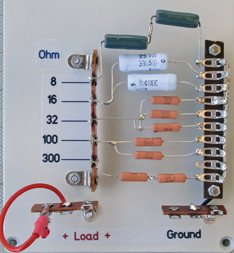
The impedance of the headphones output is 2Ω and the maximum output voltage and power depends on the connected load. I built a dummy load as shown in Photo 4 and I measured the following:
9.7Vrms 300Ω 0.3 W
9.5Vrms 100Ω 0.9 W
5.9Vrms 32Ω 1.1W
3 Vrms 16Ω 0.56 W
1.3Vrms 8Ω 0.21W
The impedance of the line output is 100Ω and the maximum voltage is 10Vrms at 2kΩ. I measured the distortion at 1kHz in all the described loads from 8Ω to 300Ω, keeping the level constant at 1Vrms. I never measured distortion above 0.001%, which unfortunately is the limit of my distortion analyzer. I am sure that the real distortion is much lower.
A very important issue that affects the quality of the stereo reproduction is the imbalance between the two channels. This is mainly due to the volume potentiometer since the gain of the preamplifier is set with high accuracy resistors. I measured this by moving the potentiometer to various positions and I noticed that the Left Channel was always greater in level than the Right Channel, from 0.15dB to a maximum of 0.3dB. I decided to increase the gain of the Right Channel by 0.22dB by soldering a resistor of 15.6kΩ in parallel to R56 (470Ω). The final result was that the imbalance between the two channels drop to ±0.1dB, at least for the positions around the middle, which are the most frequently used in listening.
The PhL-100 uses a common PCB for both channels and I took every precaution during the design and construction to avoid any interference from one channel to another. Testing the cross-talk between the channels proved that the result was successful. The test was performed at 1kHz, 10kHz, and 20kHz with the output voltage of one channel at 10Vpeak and the input of the other channel open. The results were -81dB at 1kHz, -69dB at 10kHz, and -64dB at 20kHz.
Conclusion
The PhL-100 is a versatile and easy-to-construct high-quality device. It has an input for a moving magnet cartridge and additionally two line inputs. It can easily drive every power amplifier and has a lot of power to drive almost any headphone. It is very, very quiet and offers excellent transparency. If you need such a device, I am sure you will enjoy building and listening to this one. aX
Author’s Note: I have PCBs available for the construction of the PhL-100 device. If you are interested, send me an email.
Resources
DesignSpark, www.rs-online.com/designspark/pcb-software
Front Panel Designer, www.schaeffer-ag.de
G. Ntanavaras, “The MC100 A High-Quality Moving Coil RIAA Preamplifier,” audioXpress, March 2014
https://audioxpress.com/article/the-mc100-a-high-quality-moving-coil-riaa-preamplifier
G. Ntanavaras, “A High-Quality, High-Power Headphone Amplifier,” audioXpress, June 2013
https://audioxpress.com/article/Build-A-High-Quality-High-Power-Headphone-Amplifier
This article was originally published in audioXpress, February 2022.