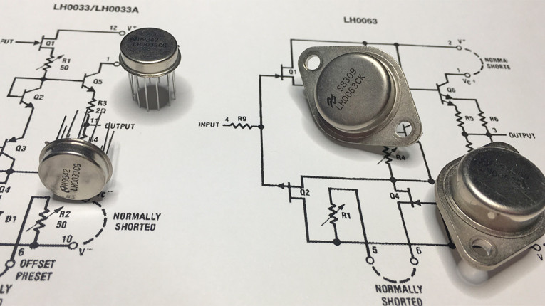
Obsolete LH0033 and LH0063 buffers were fabricated with hybrid assembly technology and built with field-effect and bipolar transistors. These buffers comprise of an input junction gate field-effect transistor (JFET) source follower and an output bipolar complementary emitter follower.
Due to the JFET input stage, these buffers may provide better isolation between input and output terminals and lower input noise current than buffers built with bipolar devices only. With the appearance of complementary JFETs from Linear Integrated Systems, it is possible to construct a discrete buffer with JFET input. The n-channel LSK189 (or the LSK489, which is dual version of the LSK189) and the p-channel LSJ289 (or the LSJ689, which is a dual version of LSJ289) are used in this design.
Circuit Description
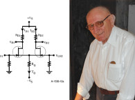
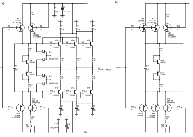
The schematic of the discrete buffer based on the LH0033/LH0063 is shown in Figure 1. The first input source follower U1A (LSK489) and the first emitter follower U3B, U5A, U5B (LS3250) provide current gain for the positive signal while the second source follower U2B (LSJ689) and second emitter follower U4B, U6A, U6B (LS3550) provide current gain for the negative signal.
The output emitter followers are biased with bipolar transistors U3A and U4A in diode connection. These forward conducting diodes also set the gate-to-source voltage in the input source followers. With gate-to-source voltage being equal to 0.6V, drain current of U1A and U2B is about 1.5mA. LSK189 (LSK489) and LSJ289 (LSJ689) are particularly suited to this circuit because of large gate-source pinch-off voltage, low capacitance, and low noise.
JFETs U1B and U2A are configured as current sources. They are adding DC current to the output current of associated input source follower. Quiescent current of the output devices is set by the current through diodes U3A, U4A. Without current sources U1B and U2A quiescent current will be 1.5mA and this value may be too low. With the value of source resistors (R1, R23+R24) about 100Ω, U1B and U2A supply additional 2.5 to 3mA, and the current through bias diodes U3A, U4A is equal to 4.5 to 5mA.
Quiescent current of the output devices can be chosen by proper selection of resistor R1, R23+R24. Variable resistor R24 can be used to adjust the current of the U1B current source. This adjustment trim DC offset between input and output and the symmetry of the output sine wave (second order distortion.) The optimal setting for zero DC offset is different from the optimal setting for minimum of the second harmonic. P-channel device (the LSJ289 or the LSJ689) has higher transconductance than the n-channel counterpart (the LSK189 or the LSK489) at the same operating conditions.
Output followers U3B, U5A, U5B, and U4B, U6A, U6B may sink or source a substantial amount of current and the voltage drop between their bases and emitters will decrease as they heat up. The bias diode U3A and the output follower transistor U3B are matched components and they share the same package.
Temperature of the bias diode is similar to the temperature of output device. This thermal tracking helps to keep nearly constant quiescent current in the output followers and prevents thermal runaway. The current through each output transistor is about 4.5 to 5mA, making the total quiescent current of the output stage equal to 15mA. Three devices are connected in parallel to ensure operation within the dissipation limit of 200mW for the SOT363 package (U3-U6). Dual diodes D1 and D2 provide the current limiting, clamping the drive to the bases of output emitter followers.
Test Results
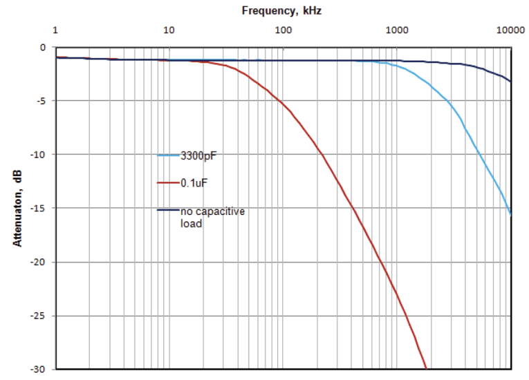
The measured buffer frequency response is shown in Figure 2. With a resistive load, the bandwidth is wider than 10MHz (about a 2dB roll-off at 10MHz, phase lag is about 30°). The bandwidth is limited by the output impedance of the JFET source followers, the collector-base capacitances of the output transistors, and the parasitic capacitance of PCB traces. The frequency response can be extended by doubling the amount of source follower devices (see Figure 1b). The penalty is correspondent rise in the input capacitance. The buffer’s input capacitance (see Figure 1a) is equal to 18 pF (the gate-drain capacitance of the input JFETs and the capacitance of PCB input trace—about 3 pF).
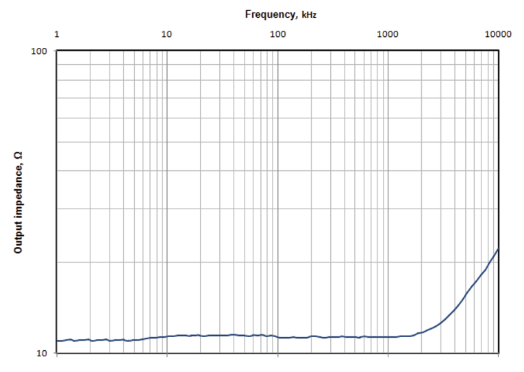
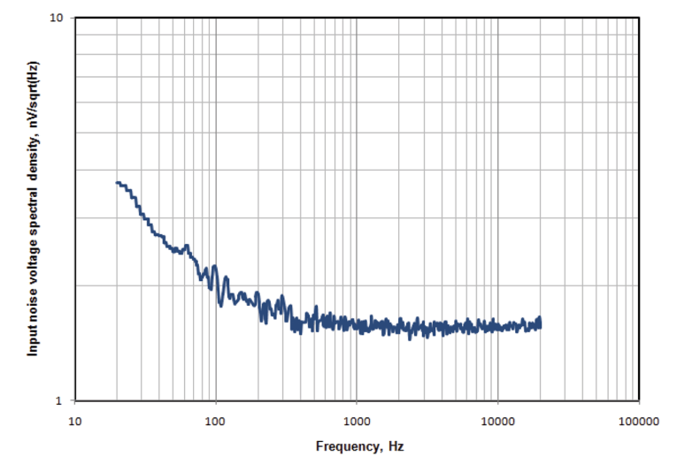
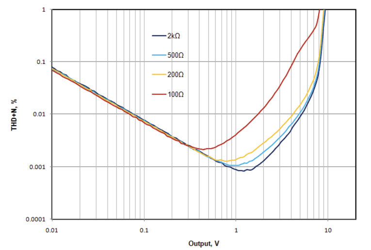
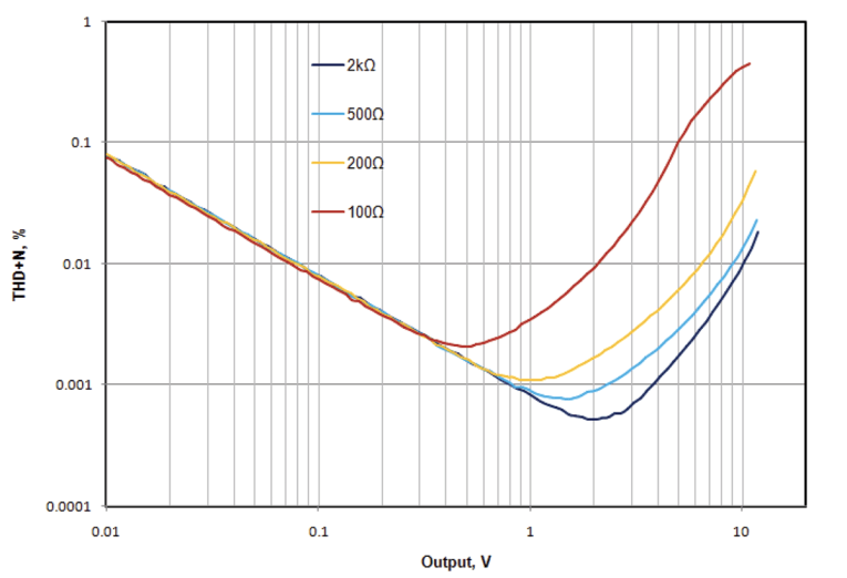
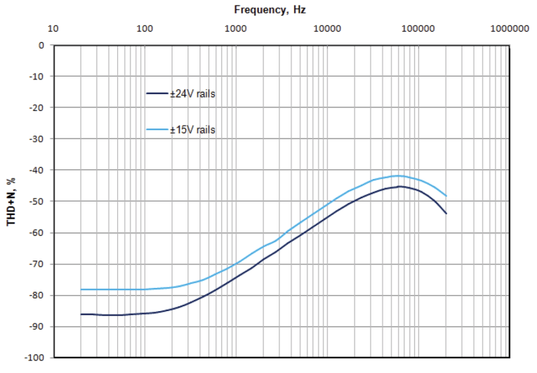
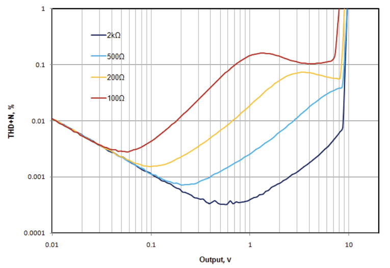
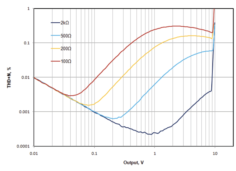
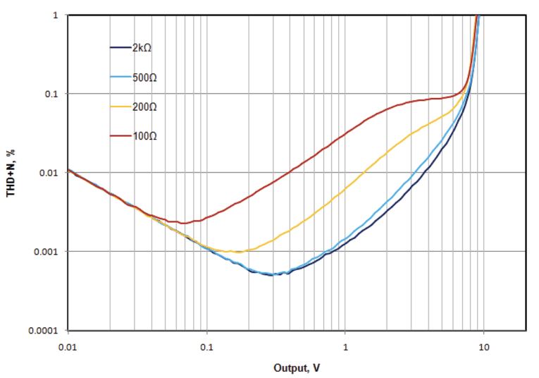
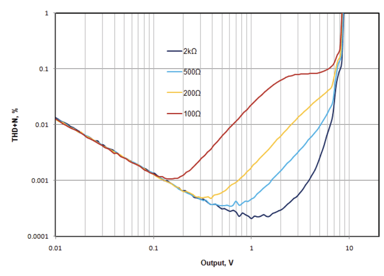
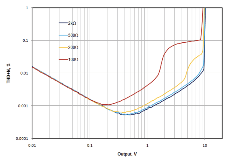
The buffer output impedance is essentially resistive (10Ω) and maintained constant up to 2MHz, as shown in Figure 3. This includes the series resistor R12 (5Ω). The series resistor may prevent parasitic oscillations with the capacitive loads. The noise voltage spectral density shown in Figure 4 is equal to 1.7nV/√Hz at 1kHz. Figure 5 and Figure 6 illustrate the unity buffer’s total harmonic distortion plus noise (THD+N) as a function of the output level for two different rail voltages.
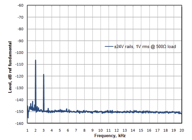
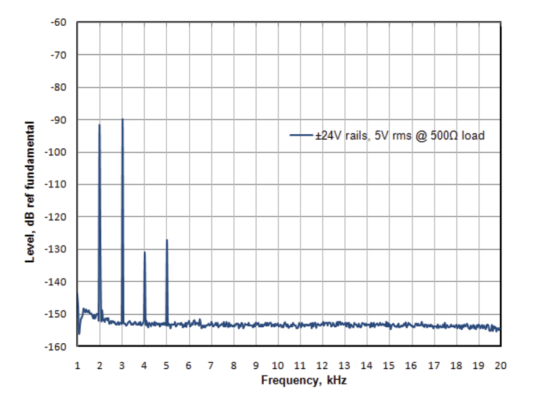
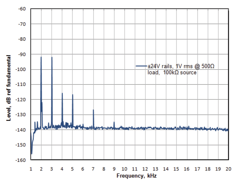
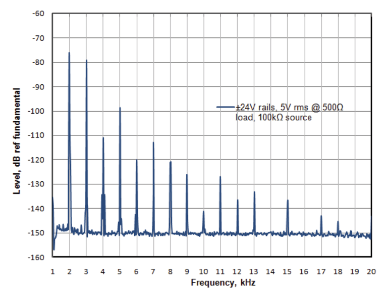
Provided distortion data were measured with low signal source resistance (50Ω). The distortion remains constant with the frequency within the 20kHz range. Typical distortion spectrums for different output voltage are shown in Figure 7 and Figure 8. The buffer input may come from a high impedance signal source. If the input impedance of the buffer is changing with the input voltage, the resulting distortion will be significantly higher than the values obtained for the low source impedance. Ideally, to preserve low distortion when operating with high source impedances, the input capacitance needs to be independent of the input voltage.
Measured distortion as a function of frequency is shown in Figure 9 for the value of signal source resistance 100kΩ. While the frequency response is flat until 100kHz, distortion increases with the rise of the frequency of the input sine wave. Distortion spectrums for different output voltage are shown in Figure 10 and Figure 11. These spectrums can be compared with the ones shown in Figure 7 and Figure 8. The input impedance nonlinearity can be improved by implementing series cascodes in the input stage (e.g., with MMBFJ310/MMBFJ176).
It is instructive to compare the performance of the proposed circuit with open-loop IC buffers. While comprehensive test results for IC buffers can be found in their corresponding datasheets (see Resources), open-loop distortion measurements are hard to locate.
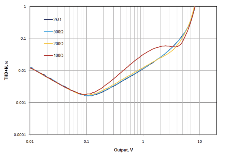
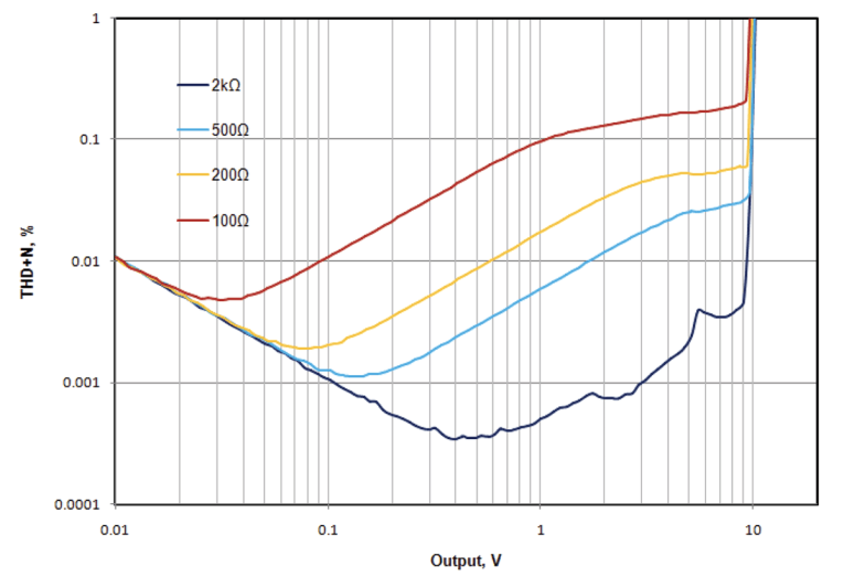
Open-loop distortion measurements for standalone IC buffers are presented in Figures 12-18. The test conditions are the same as the test conditions for measurements shown in Figure 5 and Figure 6. It is worthwhile to note that the simple circuit shown in Figure 1a produces lower open-loop distortion than many IC buffers.
Conclusion
The remarkable low distortion, wide bandwidth, low noise, and high output drive capability of the discrete buffer with JFET input allows it to be used in many audio circuits, even open loop. Among the possible applications, high-end volume control, transconductance amplifying stage isolation, line buffer, and headphone preamp come to mind. High-end volume control may consist of low impedance volume control of the designer’s choice (potentiometer, resistor ladder, transformer) isolated from signal source and the following circuit by a pair of discrete buffers with JFET input. If lower load resistance is specified, the output current capability can be increased by adding extra parallel devices to the output stage. LSK489/LSJ689 in the input stage can be replaced with MMBFJ310/MMBFJ176 at the expense of increased noise. Dual-matched bipolar devices LS3250/LS3550 can be substituted with BCM847/BCM857 or higher power PHPT610035NK/ PHPT610035PK.
The proposed discrete design outperforms off-the-shelf ICs in certain features and may serve as an economical alternative. By using various types and number of semiconductor devices, the discrete buffer can be optimized for different sources and loads. aX
This article was originally published in audioXpress, March 2019.
References
“LH0033/LH0063 Fast and Ultra Fast Buffers,” National Semiconductor, Datasheet, pp.1-14.
“BUF634 250 mA High-Speed Buffer,” Texas Instruments, Datasheet, pp.1-31.
“HA-5002 110MHz, High Slew Rate, High Output Current Buffer,” Intersil, Datasheet, pp.1-12.
“LME49600 High-Performance, High-Fidelity, High-Current Headphone Buffer,” Texas Instruments, Datasheet, pp.1-21.
“LMH6321 300 mA High Speed Buffer with Adjustable Current Limit,” Texas Instruments, Datasheet, pp.1-31.
“LT1010 Fast ±150mA Power Buffer,” Linear Technology, Datasheet, pp.1-20 Resources
“Applications for a New Ultra-High Speed Buffer,” National Semiconductor, Application Note 48, pp.1-8.
“Applications of Wide-Band Buffer Amplifiers,” National Semiconductor, Application Note 227, pp.1-22.
W. Jung, “Op-Amp Audio: Realizing High Performance: Buffers: Part I,” Electronic Design, September 1, 1998.
———, “Op-Amp Audio: Realizing High Performance: Buffers: Part II,” Electronic Design, October, 1998, pp.103-104.
R. Widlar, “Circuit output stage arrangement,” US Patent 4573021
(internals of LT1010 buffer).
S. Yee, “Complementary emitter follower amplifier biased for class A operation,” US Patent 3418589 (first complementary emitter followers in series, dating back to 1965).
 About the Author
Dimitri Danyuk has been the principal hardware engineer at Harman Luxury Audio division since 2013. He graduated with honors from Kyiv Polytehnic in 1985. His passion is to help audiophiles in all aspects of audio design. His articles have appeared in a number of magazines including audioXpress, the Journal of the Audio Engineering Society, IEEE Transactions, EDN, Electronic Design, etc. Danyuk also provides consulting services for various businesses.