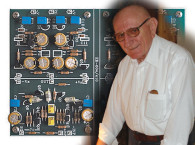
Throughout the years, Erno Borbely published several project and design articles in Audio Amateur publications (Audio Electronics, Glass Audio, Speaker Builder and audioXpress), always focusing on the lowest possible noise, best inherent linearity, and DC coupling. “Of course, all of this should always go hand in hand with the overall objective in audio: good sound,” as Borbely explained. The basic circuits on which Erno Borbely based most of his projects are described in “JFETs: The New Frontiers, Part I and II,” published in Audio Electronics AE 5/99 and 6/99, and “All-FET Line Amp,” published in audioXpress May 2002. Referring to these articles frequently, the author admits, these were the “building blocks” on which many - if not all - of his amplifiers are based. This articles continues his JFETs series and shows how you can best take advantage of JFET performance.
In Part 1 of this article, I discussed the single-stage (or single-ended) amplifier operating in common-source mode. As these stages are usually limited in audio to AC signals, the inherent DC drift is of relatively little importance. You can even use them for DC signals if you select the working point carefully at zero temperature coefficient. However, if you remember the formula for zero tempco (VGS = VP + 0.63V), you realize that the condition is different from unit to unit, since VP is different.
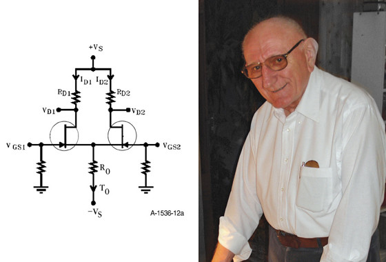
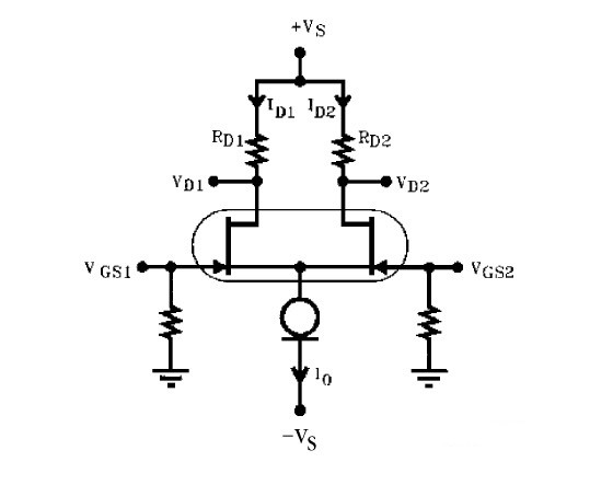
A better solution is to use a differential amplifier, where the drifts of two matched JFETs tend to cancel each other. The configuration is shown in Fig. 12a. If R0 is large enough, then:
ID1 + ID2 = I0.
Further, if ID1 changes ΔID1, then ID2 also changes by the same amount, but in the opposite direction, i.e.,
ΔID1 = −ΔID2
The differential gain of the stage is:
AV(DD) = (VD1 − VD2)/(VGS1 − VGS2) = RD × gm
which is the same as the gain of a single common-source stage. For R0 to be very large, −VS must also be very large. This is usually inconvenient, so instead of a resistor, you use a so-called constant-current source, which delivers I0 independent of −VS (Fig. 12b).
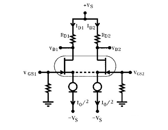
Due to its symmetrical nature, you can also consider the differential amplifier as two symmetrically arranged “half-circuits,” each with a JFET, a load resistor, and half of a current source, providing I0/2. (1) This is shown in Fig. 13. If the two JFETs are “identical,” then you can join the two half-circuits together at the sources without upsetting the DC operation. However, you now have balanced single-ended amplifiers.(2)
Seen from gate 1, JFET 1 operates as a common-source amplifier, except that the source is connected to the source of JFET 2, operating it with source input. Seen from gate 2, the same thing happens - JFET 2 is in common-source mode, driving JFET 1 in the source. There are a number of advantages to operating two JFETs in this way, and I will start here with the common-mode rejection.
Common-Mode Signals
A very important feature of the differential amplifier is its ability to reject common-mode signals. Common mode means that both gates are driven with the same polarity and equal amplitude signals. It is easy to see that if only gate 1 is driven positive, then ID1 increases and ID2 decreases. But if both gates are driven positive, then both ID1 and ID2 must increase, which is impossible because ID1 + ID2 = I0; i.e., I0 is constant. Consequently, the differential amplifier cannot amplify same-polarity or common-mode signals.
Just how good it is in rejecting common-mode signals is expressed with the common-mode gain:
AV(CM) = −RD/2r0
where r0 is the output impedance of the constant-current source. In order to have low common-mode gain (i.e., good rejection), the output impedance of the current source must be very large.
The importance of low common-mode gain is closely related to the temperature drift, because changes in ID, VGS, and gm can be considered common-mode signals if they are the same for both JFETs. Normally, a common-mode rejection ratio (CMRR) is specified for the differential amplifier. It is the ratio between the differential gain and the common-mode gain:
CMRR = AV(DD)/AV(CM) ≈ 2gm × r0.
Obviously the two JFETs must be closely matched to achieve good common-mode rejection. In fact, these two formulas are valid only if the two JFETs are perfectly matched. Although it is possible to select well-matched JFETs, the easier way is to use dual JFETs matched by the manufacturer, or even better, dual JFETs manufactured on the same silicon chip, i.e., monolithic duals.
I have been using the NPD 5566 dual N-channel and the AH 5020CJ dual Pchannel JFETs.3 However, these are not truly complementary types, as I pointed out in my article.(3) The first complementar y types on the market were the 2SK240/2SJ74 medium gm and the 2SK146/2SJ73 high gm/low-noise types. These are closely matched single devices, mounted in a common aluminum case for good thermal tracking. Unfortunately, these devices are no longer in production.
Dual Monolithic JFETs
Although there are plenty of N-channel dual JFETs on the market, complementary dual monolithic JFETs are rare. In fact, I know of only one family, the 2SK389/2SJ109, made by Toshiba. These are still manufactured and available, so I use them in all my amps with differential input. Now I’ll describe some practical differential circuits.
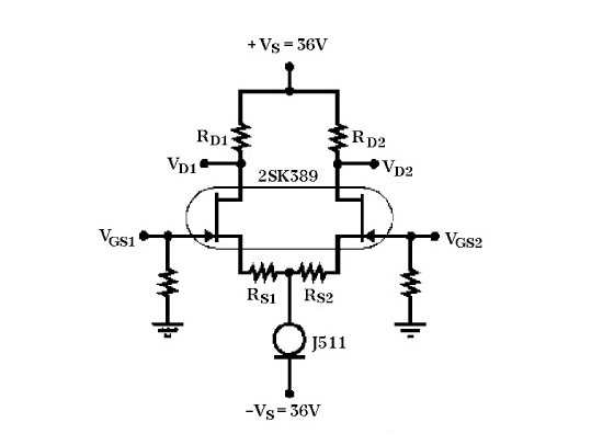
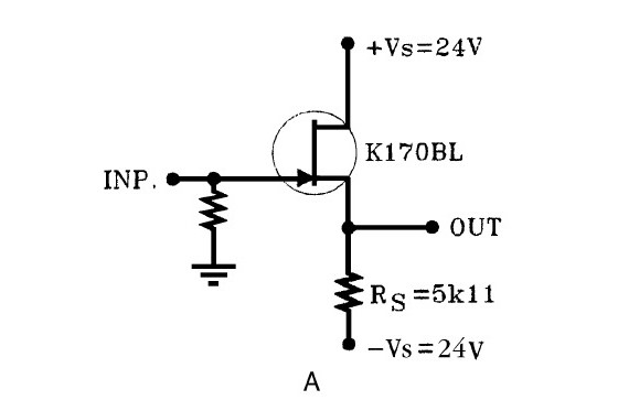
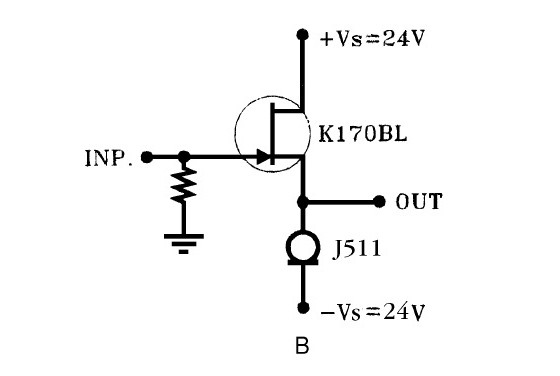
Figure 14a shows a simple differential amplifier with the 2SK389 dual monolithic JFET from IDSS group V. I hooked it up with ±36V to operate the JFETs under conditions similar to those of the SE ones. The constant-current source is a J511 JFET delivering 4.7mA. In order to run the drains at roughly one-half the supply voltage (about 18V), I chose RD1 = RD2 =10k.
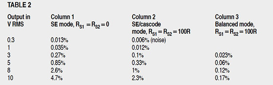
First I tested the amplifier in single ended mode, i.e., gate 2 connected to ground, with the measurements taken at VD2. (VD2 has the same phase as VGS1.) Although from the operational point of view it is single-ended, I think this mode is more appropriately called the unbalanced mode. Gain without local feedback (RS1 = RS2 = 0) is about 64 times, which is 36dB. Frequency response is 175kHz, and the input capacitance is 330pF. THD, measured at 1kHz, is shown in column 1 of Table 2.
Next I inserted source resistors RS1 = RS2 = 100R, and reran the measurements. Due to the local feedback, the gain dropped to approximately 28 times, and the input capacitance to 160pF. The THD also decreased by about 6dB.
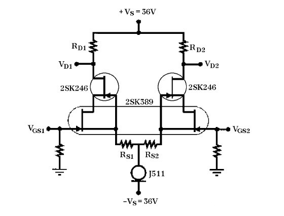
In order to reduce the input capacitance further, I put 2SK246 cascodes in the circuit (Fig. 14b). The gain did not change significantly, but the input capacitance dropped to 50pF! THD also decreased, as shown in column 2, Table 2.
Balanced Mode
A couple of comments are in order concerning this circuit. According to the measurements, it is a very decent design, considering that it uses only a very small amount of local feedback. The gain is still fairly high, and you can reduce it further by increasing the source resistors, which in turn further reduces the THD. However, to fully take advantage of the symmetrical nature of this circuit, you should use it in balanced mode, which requires applying a balanced signal at the two gates and taking the balanced signal from the two drains.
I have made some rudimentary THD measurements in balanced mode, shown in column 3 of Table 2. Unfortunately, my oscillator and THD analyzer (HP339A) are unbalanced, so I needed to improvise the balanced operation with op amps, limiting the measurements to the levels shown in the table (lower levels were masked by noise).
Nevertheless, it clearly indicates that the circuit thrives in balanced mode, having 10–20dB less THD compared to unbalanced mode. It also indicates the advantages of this circuit relative to the SE circuits discussed in Part 1.
The SE purists might naturally say that this is due to the cancellation of evenorder harmonics in the balanced circuits, which is true. But as Nelson Pass points out on his homepage, in comparison to the SE stages, the balanced circuit does not give rise to odd-order distortion. There is simply not much distortion left in the balanced circuit.
As mentioned in Part 1, the input capacitance is voltage-dependent, which can cause THD when the amplifier is driven from high source impedances. I have tested the circuit described in column 2 of Table 2 with 50k, 100k, and 500k sources. There was no measurable change in distortion up to 100k, but at 500k, I could see a slight increase.
Again, for noise reasons, you should probably keep the source impedance below 50k, so there is no problem with the capacitance modulation anyway. I also checked the CMRR by connecting the two gates together and driving them with a 3V RMS signal. The output, again in balanced mode, was down 87dB at 1kHz. The CMRR dropped to 70dB at 10kHz and 63.5dB at 20kHz, but even at 100kHz, it was 50dB!
The Output
I have now described two types of amplifier stages using JFETs, the common source or single-ended stage, and the differential or balanced amplifier. You can use either of these to build audio amplifiers, depending on your preference for balanced or unbalanced operation. Personally, I prefer the differential circuit, because you can use it with balanced or unbalanced sources, and it can also feed balanced or unbalanced power amplifiers. Balanced operation gives a subjective impression of increased dynamics. It can also be an extremely useful interfacing consideration in breaking up ground loops.(4)
There are two issues to consider when talking about the SE and balanced amplifiers. First of all, the output does not sit at 0V DC, but at some 10–20V above ground. If you wish to connect it to, say, a DC-coupled power amplifier, you must block this DC voltage from reaching the power-amp input. This is easily done using a capacitor, and this problem is well known to all SE fans, whether of tube or semiconductor variety. I will therefore not spend much time on the subject.
A much more important question is whether these circuits can drive the input impedance of a power amplifier. The output impedance of the amps examined is basically equal to the drain resistor of the amplifier. If RD = 10k, then the output impedance is also close to 10k. But if the input impedance of the power amp is also 10k, then you are certainly in trouble. First, you lose 6dB of gain by the voltage division between the 10k resistors; second, the 10k input will most likely load the output and cause a lot of THD. Even with 20k or 50k input impedance, you might run into problems. It is advisable to put an impedance transformer at the output to avoid this. Source followers to the rescue!
JFETs as Followers
Just like tubes and bipolar transistors, JFETs can also be operated as followers, more specifically source followers. The basic circuit is shown in Fig. 15a. The drain is AC-grounded, and the output signal is taken out across the source resistor, which means it operates with 100% local feedback. The gain of the source follower is:
AV = gm × RS/(1 + gm × RS)
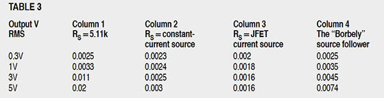
Two things become obvious from the formula: first, the source follower does not reverse the phase of the signal, and second, if gm × RS >> 1, then the gain becomes approximately unity. In order to make RS large, you can use a constant-current source with high output impedance (Fig. 15b). The linearity is also dependent on RS (see the 1kHz THD measurements in columns 1 and 2 of Table 3).
The input capacitance is low because it is not augmented by the Miller effect. I measured approximately 5pF for the circuits in Fig. 15a and b. The output impedance equals approximately 1/gm. With high-gm devices, this will be fairly low. I measured 38Ω for the basic circuits in Fig. 15a and b.
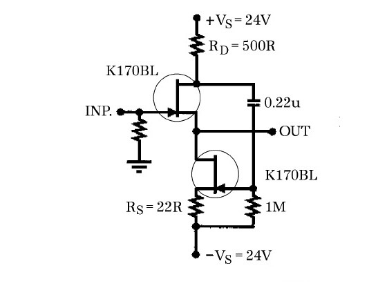
The circuits in 15a and b have a DC offset voltage at the output—the gatesource voltage at the given drain current. For the JFETs I used in the test setup, I measured a 0.2V offset. If you need zero DC output, you can use the circuit in Fig. 15c. Here the constant-current source is made with the same type of JFET as the follower.
If the two JFETs are matched and the two source resistors are equal, then the DC offset will be very small. With two matched K170BLs, I measured less than 1mV offset. (It would probably be even lower if you used here a dual monolithic JFET like the K389BL/V.) DC drifts tend to cancel out as well, because of the matched devices. The circuit also has very low THD (see column 3 of Table 3).
Follower Feature
One of the most important features of a follower is its ability to drive low-impedance loads. I checked all three circuits with 1k and 10k loads at 3V RMS output. With 1k they measured 1%, 1.7%, and 0.23%, respectively. Although its output impedance is actually higher than the circuits in Figs. 15a and b, that in 15c is better in driving low-impedance loads. With a 10k load, the circuits in 15b and 15c didn’t have many problems. THD was 0.004 and 0.0022%.
My choices of source followers are shown in Fig. 16. The circuit in 16a is a JFET version of the tube White cathode follower. (5) Basically, the circuit is an extension of Fig. 15c, in that the follower is fed with a constant-current source, but in addition the drain current of the current source is modulated by the AC signal. When the output signal goes positive, the tail current decreases, and when it goes negative, the current increases. The result is a significant reduction of the output impedance and an apparent increase in drive capability.
The output impedance with the devices shown measured 2.3Ω. The input capacitance is about 5pF, the same as the previous source-follower circuits. The penalty for the drive capability is a slight increase of distortion (see column 4 in Table 3). The THD with a 1k load and 3V RMS is 0.0095%. The necessary gate drive voltage is derived from a small resistor in the source follower’s drain circuit, and it is AC-coupled to the current source.
Power Dissipation
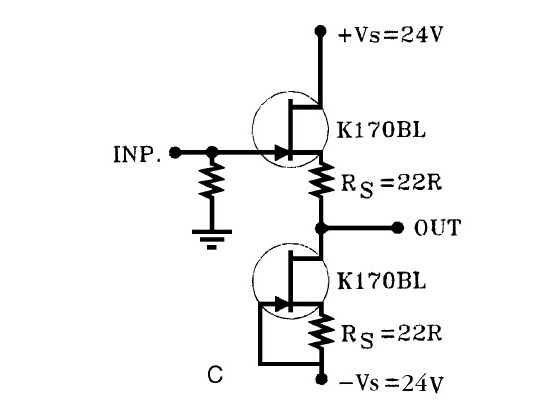
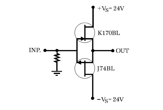
John Curl used the complementary JFET source follower shown in Fig. 16b in the JC-2 phono-preamp module. (6) The JFETs work in Class A as long as the peak load current is less than twice the bias current. After that, the circuit works in Class AB. I usually let the two matched devices work at IDSS, to maintain as much Class A headroom as possible. However, you must watch the power dissipation. If IDSS is such that the power dissipation is more than the maximum allowed, then you need to insert a source resistor to reduce the drain current or select a device with lower IDSS.
I tested the circuit with K170/J74, both the BL and V types, and got excellent results. The THD is shown in column 4 of Table 3. Depending on the matching, the offset can be as low as 1mV. The output impedance is about 18Ω, and the input capacitance is 28pF. Most important, the circuit can drive low-impedance loads without distress—the 1k/3V RMS THD was 0.0078%. With a 10k load, there is no difference from the no-load results.
I also tested the source followers for THD caused by the voltage-dependence of the input capacitance. Since the voltage excursion is much larger at the input because of the unity gain, the circuits are also more susceptible to the distortion. There is no significant increase up to a 10k source; however, at 50k the THD is increasing by an order of magnitude. Normally this is no problem, because the source impedance is usually very low. However, in certain applications such as filters, this can cause distortion.
Of course, using any of these sourcefollower buffer circuits with the SE and differential amplifiers discussed previously solves only one of the problems stated at the start of this section—the drive-capability problem. The DC voltage is still there. Given the topology of these circuits, you must use a capacitor at the output to block the DC voltage. Naturally, you can also solve this problem by using level-shifting circuits, but it requires a bit more circuit design. For now, I’ll look at an all-JFET balanced/SE all-FET line amp, using the circuits already developed.
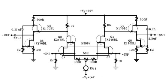
The Balanced/SE All-JFET Line Amp
The schematic shown in Fig. 17 consists of the differential amplifier Q1/Q2, cascoded with Q3/Q4, and the output buffers Q5/Q6 and Q7/Q8. The differential amplifier uses a dual monolithic K389V JFET. Each JFET operates at just over 2mA, this current supplied by the J511 constant-current source. The 330R source resistors provide local feedback and control the gain of the differential amplifier. The trimpot P1 cancels out small imbalances between the two JFETs, but it is normally unnecessary with monolithic duals, and you can leave it out.
The Cascode FETs are K246BLs. The output buffers are those I developed from the tube White Cathode Follower, shown in Fig. 16a (“modestly” called the “Borbely” source followers here). The supply voltage is ±36V. Of course, you can make the negative supply much less than 36V; the constant-current source requires only a couple of volts for proper operation. I made them both 36V to be able to try other configurations.
The output caps must be of highest quality in order to preserve the outstand-ing sound quality of this simple circuit. If you are likely to drive loads down to 1k, then the caps must be a minimum of 10μF. If you are driving normal 10k or higher loads, you can get away with a 1μF or 2.2μF cap. I tried the Hovland Musicaps, which are rather neutral, but there are plenty of good caps on the market you can try.
Normal oil caps are not for this circuit; they destroy the excellent resolution to a “nice” blurred mish-mash. (Don’t get the idea that I don’t like oil caps; I use them in some of my amps.) I would have liked to try some silver-foil caps, but, alas, the prices are more ridiculous than the cable prices, and I refuse to play that game. (If anyone knows of a reasonably priced silver-foil cap, please let me know.)
You can use the line amp with unbalanced or balanced sources, and you can feed power amps with balanced or unbalanced inputs. However, you should really take advantage of its superior performance in balanced operation, as I mentioned before. Should you use it with unbalanced sources, then you must short the –INP to ground. And in the unlikely event that you don’t wish to take advantage of the balanced outputs, you can leave out the circuit around Q5/Q6, i.e., the negative output. I recommend a 10k or 20k ladder attenuator as a volume control.
Good luck with the JFETs, the “New Frontiers” in audio amplification.
References
1. Erno Borbely, “New Devices for Audio from National Semiconductor,” Audio Amateur 5/83, p. 7.
2. Nelson Pass, www.passlabs.com.
3. Erno Borbely, “Third Generation MOSFETs: The DC-100,” The Audio Amateur 2/84, p. 13.
4. Walt Jung, private communication.
5. Erno Borbely, “Differential Line Amp with Tubes,” GA 1/97, p. 24.
6. John Curl, “Classic Circuitry,” The Audio Amateur 1977, Issue 3, p. 48.
Acknowledgments
Many thanks to Walt Jung of Analog Devices for his valuable comments and suggestions.
This article was originally published in Audio Electronics, Vol 5 1999
About the Author
Erno Borberly was employed by National Semiconductor Europe for more than 20 years. He was Manager of Technical Training and worked as a consultant in human-resources development. He received an MSc degree in Electronic Engineering from the Norwegian Institute of Technology, University of Trondheim in 1961, and worked seven years for the Norwegian Broadcasting Corp. designing professional audio equipment, both in tube and in semiconductor technology. In 1969 he moved to the US and was Director of Engineering for Dynaco. He was named Director of Engineering for Dynaco in 1972, where developed the Cascode output stage for the Stereo 400 power amplifier, and the Dynatune circuit for the FM5 FM tuner, for which he received a US patent.
From 1973–1978, he worked for Motorola, as Senior Applications Designer and Applications Manager. There he developed power amplifiers, low-noise preamplifiers, and FM tuners. Some of this work was put to good use, when he joined the David Hafler company in 1978 as Director of Engineering. Mr. Borbely developed the DH101 preamplifier and the DH200 power amplifier, which was the first one to use MOSFETs in the US.
When retired from National, Erno Borbely and his wife Irene started Borbely Audio, which sold high quality kits to end-users. Since 1982 he published his designs in Audio Amateur/Audio Electronics, Speaker Builder, Glass Audio, and audioXpress.
More about Erno Borberly