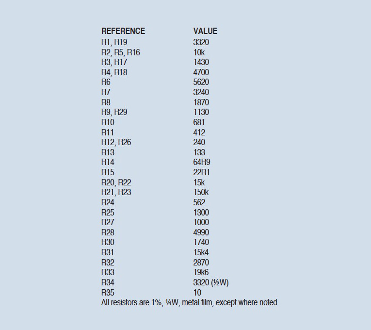
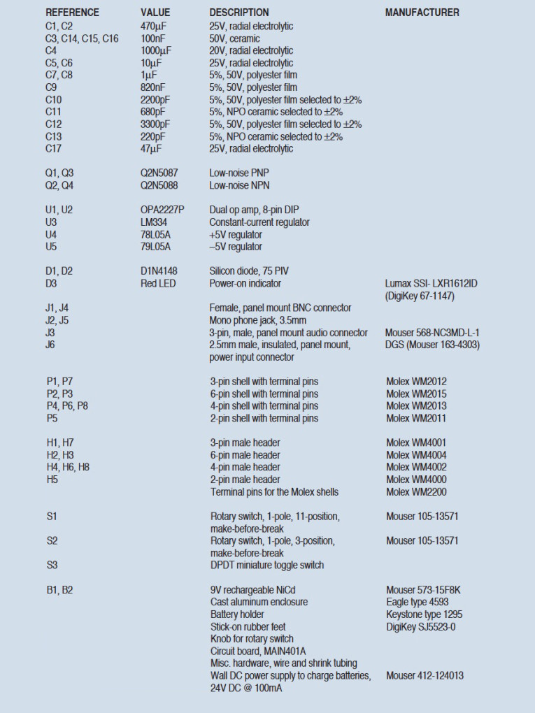
Input Stage Design
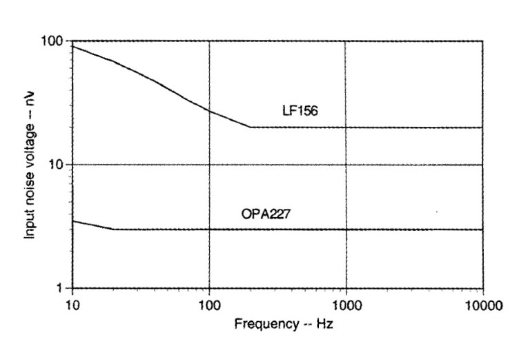
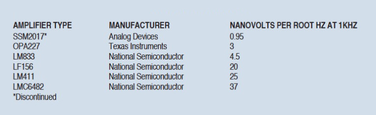
The first step was a data book search to find solid-state amplifiers with a low input noise voltage (Table 1). The l/f noise, so-called because its spectral density increases as the frequency decreases, is a curve for each amplifier (Fig. 1). However, the “spot” value at 1kHz is a good indicator of a low noise device, as is the so-called “corner frequency,” that is, the frequency at which the noise voltage sharply increases. A low corner frequency is better because there is less total noise within the audible range.
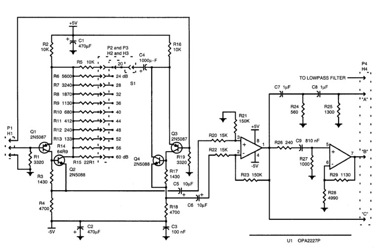
From Table 1, the SSM2017 looks like a good choice for the input stage, but unfortunately the manufacturer has discontinued it. The second table entry, the OPA227, looks pretty good, but I decided to first try to duplicate the input configuration of the SSM2017 with discrete transistors to see how well I could do. A data book search for high gain, low noise transistors led me to the 2N5087 (PNP), and 2N5088 (NPN), which I could use in a compound pair for much better linearity than I could get from a single transistor (Fig. 2). The 2N5087 data sheet (2) has a graph of wideband noise figure contours as a function of source resistance and collector current. A collector current of about 400μA looks as though it would minimize the noise in the source resistance range — 150 to 600Ω — that matches most dynamic and buffered capacitor microphones.
I had already decided on a fully metal enclosure with internal rechargeable batteries to minimize unwanted signal pickup. I could regulate the ±9V from the batteries to working voltages of ±5V. After a few rough calculations I had starting resistor values that I could use in a SPICE model to optimize my design. The SPICE program steps resistor values to minimize the output noise. The final circuit values are shown in Fig. 2 and in the parts list (Table 2). The SPICE output file lists the 2N5087 collector current as 400μA and the 2N5088 collector current as 360μA. (This design may not be truly optimum, but real component tolerances make it impractical to tweak out the last few percent!) I also decided to build the same preamp with an OPA227 input stage, which I call a model 401B, to see whether the discrete transistor design effort had been worthwhile (Fig. 3). I call the discrete transistor version a model 401A, because this makes the test results easy to label.
The Rest Of The Design
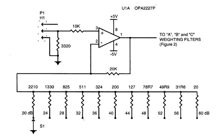
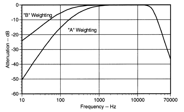
I chose a gain range of 10 to 1000 (20 to 60dB) in 4dB steps because 11-position rotary switches are common and because I seldom need a gain of less than ten. I included “A” and “B” frequency weighting filters as well as a flat (“C”) response because they are sometimes useful and their addition didn’t cost much. The networks use only a few components and the measured response curves are within limits (Fig. 4).
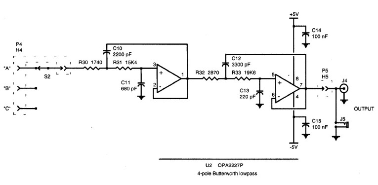
The output stage in Fig. 5 is a 4-pole Butterworth low-pass filter with a cutoff frequency of 25kHz. This reduces the high-frequency noise from the previous stages and may help reduce the noise aliased into the passband when driving a sound card’s line-input.
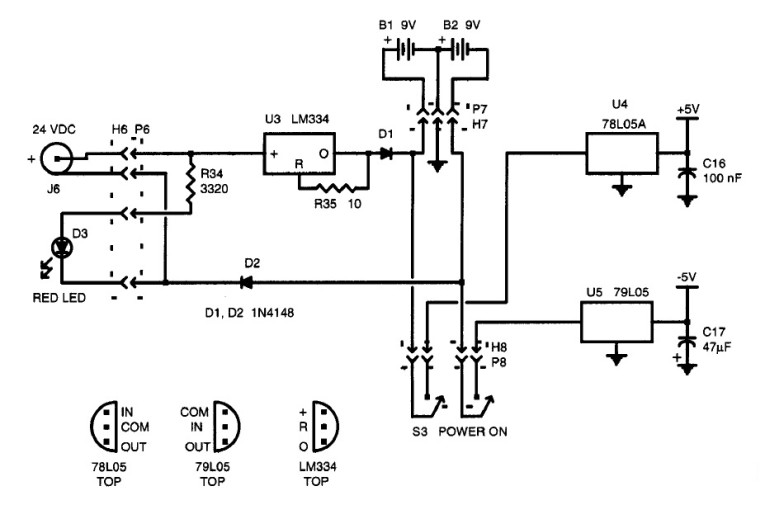
Figure 6 shows the power-supply circuit, which consists of a 10mA constant-current battery charger and the ±5V regulators. This current is low enough so you can leave the batteries on trickle charge all the time when the preamp is not in use. You can, of course, use the preamp with the charger connected, but you may get better isolation with it disconnected. The battery current is so low the preamp will run for many hours on a full charge.
Construction
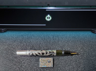
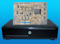
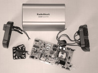
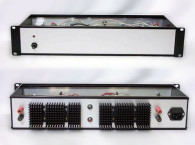
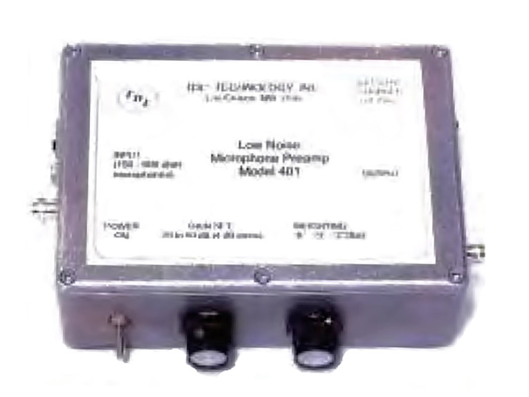
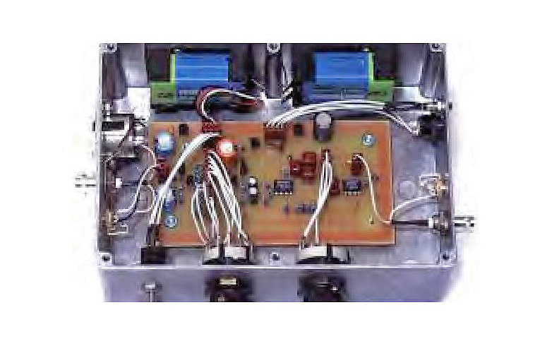
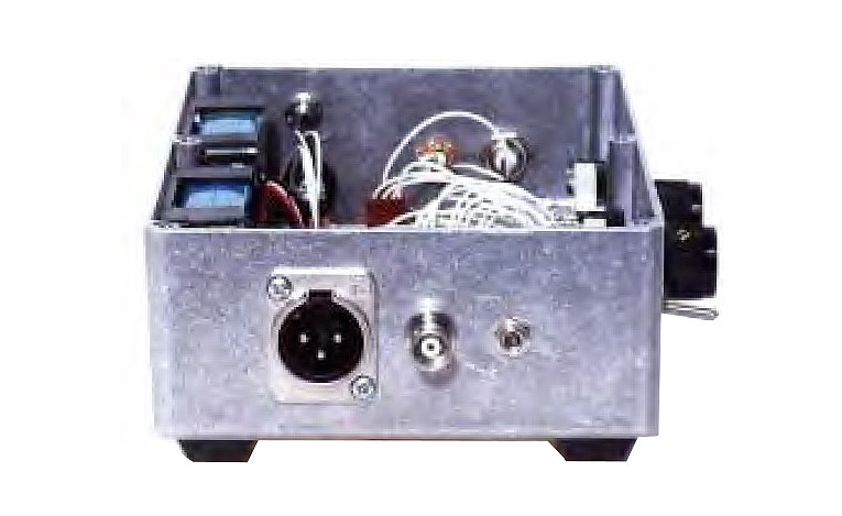
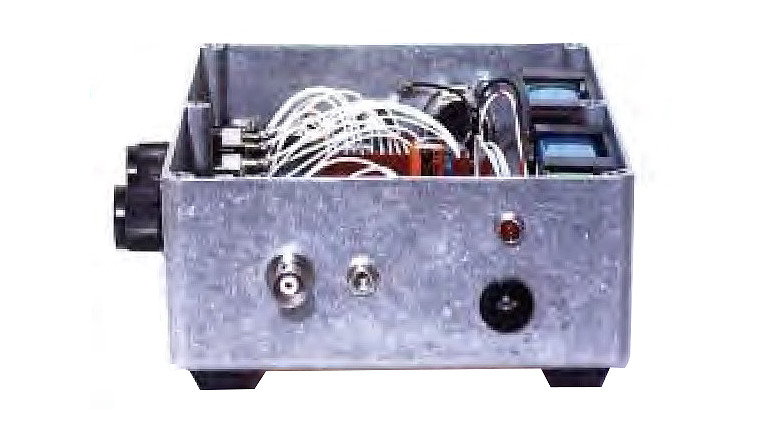
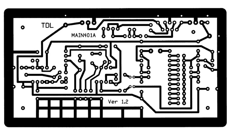
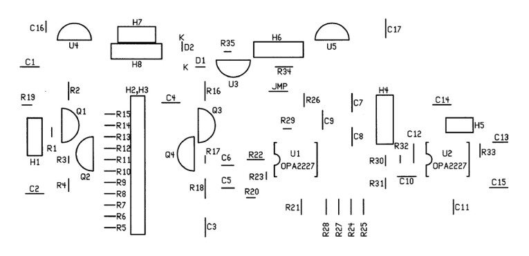
Construction is straightforward. As shown in Photos 1, 2, 3, and 4, all components except the batteries, connectors, and switches are on the single-sided printed circuit board (Figs. 7 and 8). I used three different input connectors and two output connectors because I find it convenient to not have to search for adapters. Switch and connector placement is not critical, and you can use the photos as a drilling guide.
The cast enclosure is easy to drill because the hard aluminum alloy cuts cleanly. All connections to and from the circuit board are made with Molex male headers on the board and mating plugs. I mounted the board on the bottom surface of the enclosure using four 4-40 × 5/8" machine screws, four internally threaded 3/8" long nylon spacers, and four 4-40 hex nuts. Actually, only one or two nuts are needed, because the wiring helps hold the board in place. When the top cover is attached with its six screws, the result is a compact, well-shielded module.
Performance Testing
When testing an amplifier with a sound card, it’s useful to put an attenuator between the signal source and the amplifier’s input so you have an overall gain of unity. You still have the same amplifier input voltage, but the higher level into the attenuator is much easier to set.
The spectral graphs in Figs. 9–13 were made with shareware program At-SpecPro (4) and checked with a Hewlett-Packard Wave Analyzer model 3581A. This analyzer has a 90dB single-scale range and a total dynamic range of over 200dB, which is sufficient for testing this preamp.
Although very low distortion audio signal generators are available, they are expensive compared to using software and a sound card. I used a freeware program named Wavetools (5) to generate the tones for the intermodulation distortion tests. Just start the signal generator program twice and set the frequencies and output levels as needed. If you have enough computer memory, you can start this program multiple times to produce a wide spectrum of tones.
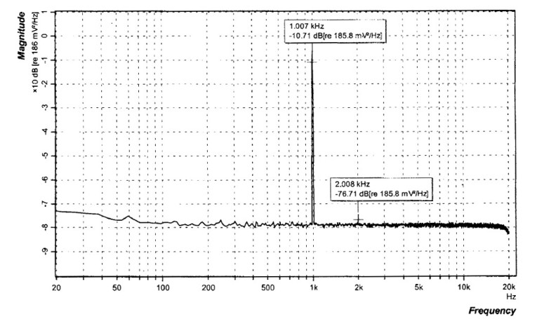
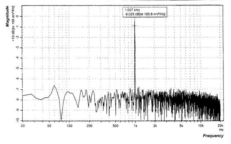
Figure 9 shows the model 401A output spectrum at 60dB gain and flat or “C” weighting. The 1kHz output amplitude is just below the maximum sound card line-in level, and you can see that the usable dynamic range is nearly 70dB. The only harmonic visible is the second, and it is down 66dB, which is a THD = 0.05%. (The H-P Wave Analyzer read 0.032%.) The small 60Hz “line” would disappear if either “A” or “B” weighting were used; the flat response is worst case at low frequencies.
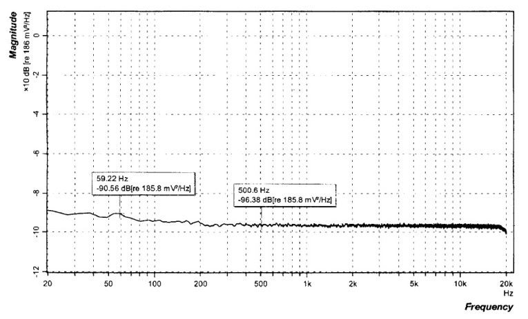
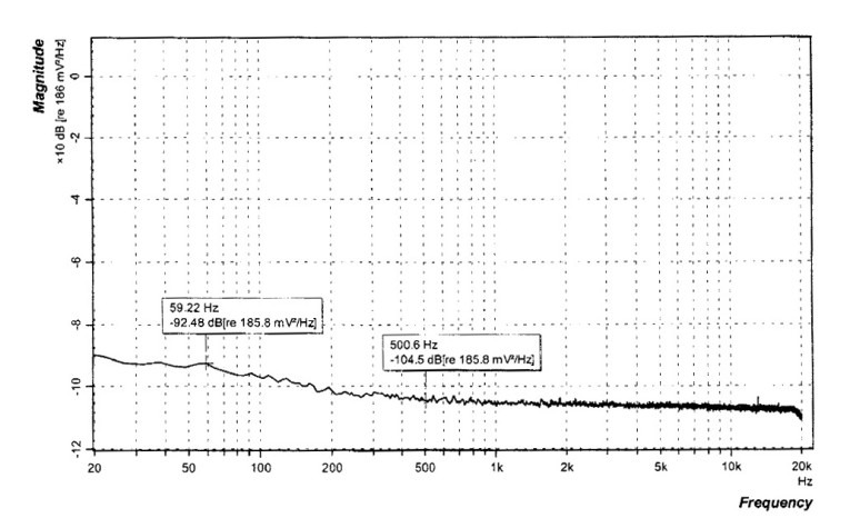
As the preamp gain is lowered, the noise floor goes down and the dynamic range increases. The floor is down to about −96dB at 40dB gain (Fig. 10), and it’s down to less than −100dB at minimum gain the sound card’s input shorted looks the same as Fig. 11. In Fig. 12 you can see the model 401B response for the same test conditions. The noise floor is about 10dB higher so the dynamic range is 10dB lower. Clearly the discrete transistor input performs better.
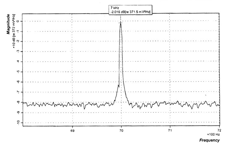
Figure 13 shows the output spectrum of an intermodulation distortion test on the model 401A. I used a 7kHz sine wave with a relative amplitude of unity summed with a 90Hz sine wave with an amplitude of 0.1 as the input. No IM products are visible. Nor were they visible for the model 401B, but the noise floor was higher.
So how does it sound? Well, it’s very quiet. I connected a Sony condenser mike to the preamp’s input and the preamp output to the input of one of my sound systems. With the mike off, the sound system gain at maximum, and the preamp gain at 44dB or lower, I couldn’t hear anything out of the speakers. At 48dB I heard a faint hiss if I turned off the fluorescent lighting. At 60dB the hiss is barely audible. Recordings are very clean with a lot of dynamic range.
Final Thought
I am very pleased with the results of this project and I think you will find it worth your time and expense to build one. If there are any updates to the design, I will post them on my website for you to download.
Glossary
Aliased — When an analog waveform is sampled at less than twice its maximum frequency, the higher frequencies are translated down or aliased into the sampled data.
Dynamic range — The difference in amplitude level between the maximum and minimum useful signals. The maximum level is limited by the overload point of the device under test or the sound card. The minimum level depends on the noise floor.
Intermodulation distortion (IM) — The mixing of two or more pure tones in the device under test to produce sum and difference tones. IM is primarily a test for nonlinear distortion at the highest test frequency.
Noise floor — The residual system noise. Called a noise floor because you can’t see any signal with a lesser amplitude.
Total harmonic distortion (THD) — Nonlinearity in the device under test produces harmonics of the test signal. That is, a 1kHz tone would have harmonics at 2kHz, 3kHz, and so on. THD is the square root of the sum of the squares of all measurable harmonic voltage levels. THD can be expressed in dB with respect to the fundamental level or as a percentage of the fundamental level. aX
This article was originally published in audioXpress, October 2002.
References
1. “Sample Champion Pro” version 2.5, by Paolo Guidorzi for Microsoft Windows 95 or higher.
2. 2N5087 data sheet from ON Semiconductor. Download the pdf file from http://onsemi.com.
3. Simulation Program with Integrated Circuit Emphasis (SPICE). I use TopSPICE Plus from Penzar Development, but any of the commercial products should work fine.
4. You can download “AtSpecPro” version 2.2 by Paavo Jumppanen from www.taquis.com. The unregistered version has somewhat limited performance but will give you a feel for its capabilities.
5. Download “Wavetools” from www.mda-vst.com. It’s freeware!
Check the next page for a review of the TDL Model 401 Microphone Preamp and Ron's further comments.