
“The Lattice Nexus platform augments the parallel processing and re-programmability of FPGAs with the power-efficient performance demanded by today’s technology trends, like AI inferencing at the Edge and sensor management. The platform also accelerates the rate at which Lattice will release future products,” explains Steve Douglass, Corporate Vice President, R&D, Lattice Semiconductor. “Additionally, the Lattice Nexus platform offers easy-to-use solution stacks targeting high-growth applications that help users more quickly develop their systems, even if they are not experts in FPGA design.”
To increase ease-of-use, the Lattice Nexus platform provides new system-level solutions that combine design software and pre-engineered soft IP blocks with evaluation boards, kits and reference designs to enable developers to build their systems more quickly. These solutions target key growth application areas, including sensor bridging, sensor aggregation and image processing.

The Lattice Nexus platform introduces innovative architectural features that optimize system performance at industry-leading low power, including optimized DSP blocks and higher on-chip memory capacity. These features enable power-efficient computing, such as AI inferencing algorithms, running twice as fast at half the power of Lattice’s previous FPGAs.
Lattice Nexus also uses an innovative circuit design to deliver key capabilities, including programmable power-performance optimization and very fast configuration for instant-on type applications. The new generation FPGAs are developed on high-volume 28 nm fully-depleted silicon-on-insulator (FD-SOI) process technologies from Samsung, featuring 50 percent lower transistor leakage compared to bulk CMOS.
New Lattice CrossLink-NX FPGA
The first FPGA developed on the new Lattice Nexus FPGA platform is the CrossLink-NX, a new low power, small form factor, and high performance solution for developers working in edge computing, AI solutions for any application field, including consumer systems.
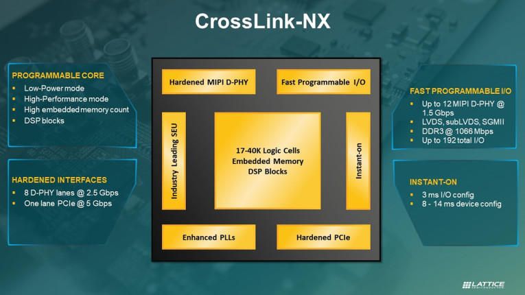
“Not only does CrossLink-NX lead in power consumption, form factor, reliability and performance in comparison to similar competing FPGAs, it is also supported by a robust library of design software, IP blocks and application reference designs,” says Gordon Hands, Director of Product Marketing, Lattice Semiconductor. “These make it quick and easy for developers to integrate CrossLink-NX FPGAs into new or existing Edge designs.”
Originally scheduled for availability in 2020, Lattice is releasing CrossLink-NX ahead of schedule and is already sampling devices with select customers.
www.latticesemi.com