
Rds(on)
Suppose you want to turn a MOSFET fully on for minimum voltage drop across it, for instance to use it as a switch. You will find that you can’t turn it on to the point where the voltage drop between drain and source becomes zero, as in an ideal switch. The higher you make Vgs, the lower the voltage drop at a given current, but there’s a non-zero limit, which is defined as Rds(on). Depending on the type and construction of a MOSFET, Rds(on) can range from a few 100Ω to less than a milliohm. It is responsible for the on-state dissipation in the device when used as a switch; with an Rds(on) of 1Ω and a current of 10A that’s 10W loss right there. In applications like switched-mode power supplies or Class-D amplifiers where the output devices are used as alternating switches, Rds(on) is an important efficiency parameter.
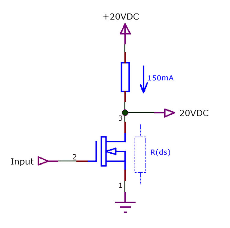
It is important to realize that there is always an Rds for an operating MOSFET, which simply is Vds/Ids. If you have an amplifier stage where a MOSFET has a Vds of 20V and carrying an Ids of 150mA, Rds is 133Ω and the dissipation in the device is 3W (Figure 1). So, there’s always an Rds but we only call it Rds(on) in the limiting case where we want to switch the MOSFET on hard, as a switch. Clearly, Rds(on) is irrelevant in a linear application.
Heat and Temperature
That Rds means there is heat dissipation in the MOSFET of Vds*Ids Watts. We all know that a semiconductor device has a limit on the maximum temperature it can work at reliably and within specs. This limit pertains to the temperature of the actual device die or junction, however, deep inside the case.
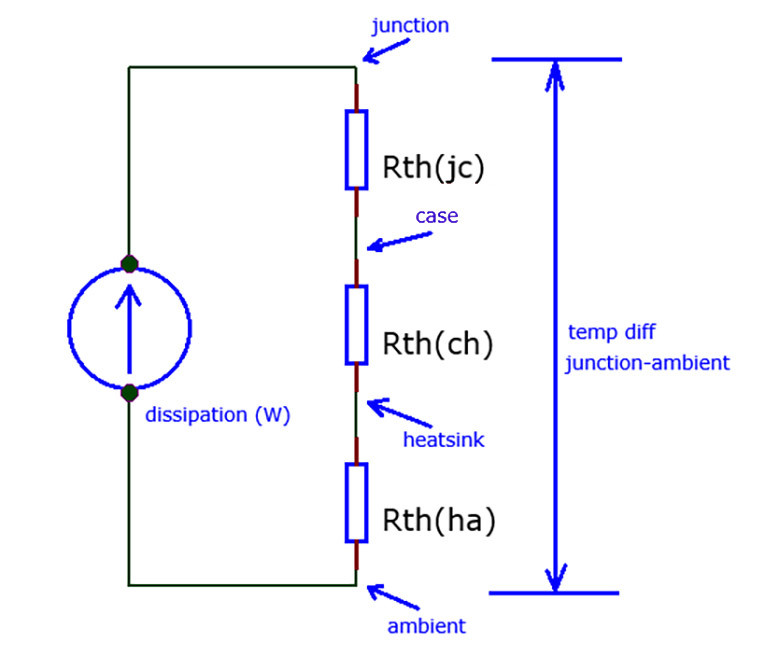
A great equivalent way to consider these issues is to look at the junction temperature as a voltage. The voltage is equivalent to the temperature - the higher the dissipation in Watts, the higher the temperature and the higher the voltage of our imaginary voltage source. Heat needs to be bled off to the outside world, to the ambient air, directly or via a heatsink.
There is a “thermal resistance” between the device junction, where the heat is produced, and the outside world. If you consider the temperature of the junction as an equivalent voltage, the path to bleed off the heat is equivalent to an electrical resistance. The analogy is so good that you can use standard electrical engineering terms and methods to calculate the actual temperatures and how much heatsinking you need.
If you look at the datasheet of a typical MOSFET, you’ll see specifications for thermal impedances, normally as degrees Celsius per Watt or C/W. Considering the temperature as an equivalent voltage, and the dissipation in Watt as an equivalent current supplying the power to increase the temperature/voltage, C/W is equivalent to Volts/Amperes and that, as Mr. Ohm has taught us, is resistance. All good so far.
An Example
We have a TO-220 device that dissipates 3W. The datasheet says it has a thermal resistance, denoted as “Rθ”, between the junction and the case (denoted as RθJC) of 16.7C/W [1]. That means that the junction will be 3W x 16.7C/W = 50.1C hotter than the case temperature. You cannot directly lower the junction temperature – the only way is to lower the case temperature, which will bring the junction temperature down, but it will always be 50.1C hotter than the case.
But there’s more. The case will also heat up because there is a thermal resistance between the case and the ambient temperature. That thermal resistance depends to a large extent on the size and shape of the case; it is clear that a large TO-247 case can shed its heat to ambient air (or a heatsink) much easier than, say, a plastic TO-92. For a TO-220, the thermal resistance case to ambient air (RθCA) is only specified indirectly for this example device as RθJA - junction to air - as 23.9 C/W. Since the thermal resistance junction to case is 16.7C/W, subtraction gives thermal resistance case to ambient of 7.2C/W.
In our example where we need to shed 3W, the case would rise 7.2C/W x 3W = 21.9C above ambient. Adding the temperature rise of junction to case to the rise of case to ambient means that the junction will operate at 50.1C + 21.9C = 72C above ambient. So, with ambient air at say 25 degrees, the junction will be at an absolute temperature of 97 degrees. Most semiconductor junctions will be OK at this temperature. But what if ambient rises to 35C on a hot day, and/or when we put the device in a box that internally has a temperature of 15 degrees above ambient? All these temperature increases will, to a first order, also raise the junction temperature and our equipment may well become unreliable.
Heatsinks to the Rescue
A good heatsink has a large surface (hence the fins) to be able to transfer heat to ambient air efficiently, meaning they have a low thermal resistance. Medium large heatsinks can have thermal resistances from their surface to ambient air of 1C/W or even lower. This means that for every Watt of thermal “load” to this heatsink, its surface will rise just 1 degree in temperature above ambient.
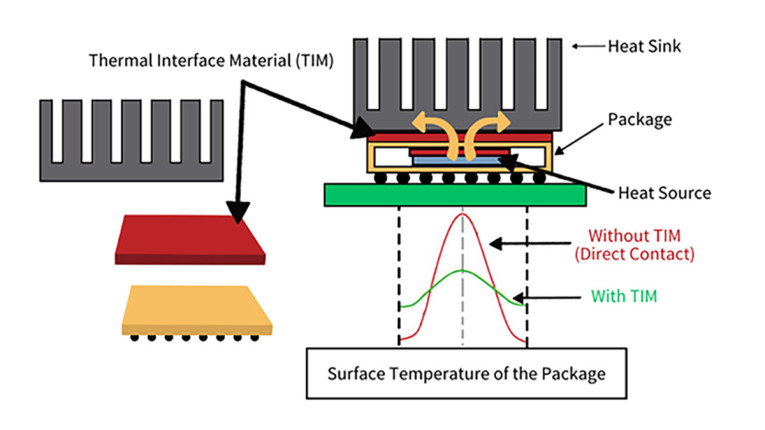
Staying with our TO-220 example that dissipates 3W, if we bolt that case to this 1C/W heatsink, the heatsink temperature rise will be just 3 degrees above ambient air, and with it the case that is bolted to it. But we need to add one more variable to the picture (Rθch, Figure 2): the thermal resistance between the TO-220 case and the heatsink surface. We usually use an isolation pad or sheet between the TO-220 case and the heatsink for electrical isolation, and such a pad also has a thermal resistance. Figure 3 illustrates the principle and shows how a good thermal interface changes the temperature distribution.
For example, a 1mil thick Al2O3 isolation pad has a thermal resistance of 0.13C/W [2]. Small compared to the other thermal resistances in the discussed example, but in other situations it can become significant so we should take it into account. (Note that TO-220 cases with a fully isolated mounting surface, also called FullPak, do not need the isolation pad but the thermal resistance of their isolating jacket is much, much higher. Their use is generally limited to switching applications where dissipations are low).
Recap
Let us revisit Figure 2. We have a heat source producing 3W. That source is connected to ambient air via the following thermal resistances: junction to case: 16.7C/W; case to heatsink: 0.13C/W; heatsink to ambient: 1C/W; or a total of 17.83 C/W from the junction to ambient air. The temperature rise from the 3W “current” through that 17.83 C/W “resistance” is 53.5 degrees. Assuming an ambient temperature of 25C, we can now say that the junction of that device will be at a temperature of 53.5 + 25 = 78.5 degrees. Most devices can reliably function at over 100 degrees junction temperature, so we have some leeway here. We could try to save some money and/or space by using a smaller heatsink. A smaller heatsink with 2C/W thermal resistance will raise the junction temperature only 3 degrees further to 81.5 degrees.
But, as mentioned, on a hot day, or inside a hot enclosure, the ambient that the heatsink connects to can be much hotter and that directly means a hotter junction and the device may get too close to its maximum operating junction temperature for comfort. For reliability, maybe we should stay with the 1C/W heatsink.
The numbers I used in these examples depend on an assumed situation and a specific device. When doing thermal design, consult datasheets for the devices, heatsinks, and accessories, and try to develop an estimate for the worst-case ambient temperature in which the device will have to function. aX
References
[1] TI LM78xx family datasheet https://www.ti.com/lit/ds/symlink/lm340.pdf
[2] P. Kwan, “Design considerations for a Class A amplifier enclosure,” Linear Audio, Volume 3, https://linearaudio.net/sites/linearaudio.net/files/v3%20euvl.pdf
This article was originally published in The Audio Voice newsletter, (#482), August 29, 2024.


