
There are several benefits to using contemporary junction field effect transistors (JFETs), which have noise voltages (Vn) equal to those found in low-noise bipolar junction transistors (BJTs). JFETs also have considerably lower noise current (In) and outperform bipolar transistors on low-frequency noise at source impedances of several kilohms and above. JFETs are also more linear than bipolar devices due to their square law transfer characteristics compared to the exponential transfer characteristics in BJTs. JFETs can tolerate higher input signals and not rely so much on the feedback to correct distortion.
Input signals can contain substantial out-of-band components (e.g., ultrasound noise ”from over-sampled noise-shaping DACs, interference from switched mode power supplies, RF from cell phones, Wi-Fi, Bluetooth devices, etc). If the input device is nonlinear, these out-of-band signals can be rectified. As a result, an unwanted envelope of rectified waveform appears at the output in addition to the desired signal. BJTs have forward-biased base-emitter junctions and JFETs have a reversed (or zero) biased p-n junction. This fact, together with exponential transfer in BJTs explain why BJT devices exhibit greater susceptibility to out-of-band signals compared with JFETs.
Another distinct difference between the BJTs and the JFETs is that the input control variable for a BJT is a current, while for the JFET, it is a voltage. JFETs do not need a biasing current for normal operation and generally don’t require DC blocking capacitor to prevent affecting the DC biasing current from the previous stage or from the signal source.
A JFET has an input voltage noise closely related to the Johnson noise of the conducting channel:

where gm is the transconductance:


The Vn in JFETs will be lowest when the devices are operated at zero Vgs (Id = I dss) or slightly positive Vgs, where transconductance (gm) is at its highest value. This will be true only if device dissipation is moderate in relation to the heat dissipation capability of the JFET package. It is also important to maintain drain-gate voltage well below the gate current (Ig) breakpoint.
A JFET input current noise is proportional to frequency:


Low-Noise Measurement System
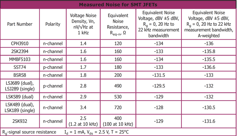
We measured voltage noise under consistent conditions using a low-noise measurement system. Id was set at 1mA, Vds was 2.5V, and ambient temperature T was 25°C. The thermal resistance of the SOT23 package is about 200°C/W, so the 2.5 mW power dissipation gives negligible rise of junction temperature. As in my original article (see Resources), we measured 16 samples of each device and averaged the noise data from 20Hz to 20kHz of 1/f and thermal noise. The curves shown in Figure 1 illustrate input noise density for various devices. Measurements of equivalent noise voltage are described in Table 1.
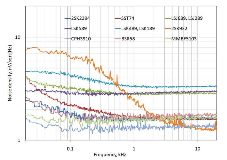
Two new n-channel devices from ON Semiconductor exhibited voltage noise densities from 1.5 to 2 nV/√Hz: the ON Semiconductor CPH3910 and the ON Semiconductor 2SK2394. Another high transconductance n-channel JFET from ON Semiconductor has significant low-frequency noise, but can be used successfully at the frequencies above 5 kHz is the 2SK932. A long-awaited p-channel device from Linear Systems, the LSJ74/SST74, has 1.7 nV/√Hz noise. All these JFETs are high-gain devices with moderate drain current (Id = 5 to 40 mA, gm = 10 to 40 mA/V).
Another three JFETs from Linear Integrated Systems — the LSJ689/LSJ289, the LSK589, and the LSK489/LSK189 — showed higher noise in the range 2 to 3nV/√Hz. These devices have moderate transconductance from 4 to 10 mA/V.
It should be noted that two measured devices from On Semiconductor — the MMBF5103 and the BSR58 — don’t have noise data in their datasheets. This means that the manufacturer doesn’t control noise parameters for these devices. The MMBF5103 and the BSR58 are designed for low-level analog switching and were included in this study for educational purposes.
Noise performance of several low-noise discrete JFETs appeared on the market in recent years was measured. The tests were done in the same way as in the first part of the article that I wrote five years ago for Electronic Design (see Resources) so that designers can make a fair comparison and select a proper part for their applications. aX
This article was originally published in audioXpress, December 2018
Resources
D. Danyuk, “Measurements Rate SMT Low-Voltage JFETs Under Consistent Conditions,” Electronic Design, April 2013,
Sources
Linear Systems: LSJ74, SST74, Ultra Low Noise, Single P-Channel JFET
Linear Systems: BSR58: N-Channel Low-Frequency Low-Noise Amplifier
Linear Systems: LSJ689 Low Noise Low Capacitance Monolithic Dual P-Channel JFET Amplifier
Linear Systems: LSK589 Low Noise, Low Capacitance Monolithic Dual N-Channel JFET
Linear Systems: LSK489 Low Noise, Low Capacitance Monolithic Dual N-Channel JFET Amplifier
ON Semiconductor: CPH3910: N-Channel JFET, 25 V, 20 to 40 mA, 40 mS, CPH3
ON Semiconductor: 2SK2394 N-Channel JFET
ON Semiconductor: MMBF5103 N-Channel Low-Frequency Low-Noise Amplifier
ON Semiconductor: 2SK932 N-Channel JFET
 About the Author
Dimitri Danyuk has been the principal hardware engineer at Harman Luxury Audio division since 2013. He graduated with honors from Kyiv Polytehnic in 1985. His passion is to help audiophiles in all aspects of audio design. His articles have appeared in a number of magazines including audioXpress, the Journal of the Audio Engineering Society, IEEE Transactions, EDN, Electronic Design, etc. Danyuk also provides consulting services for various businesses.