Toshiba Semiconductors manufactured many junction field-effect transistors (JFETs) for audio applications: the 2SJ74/2SK170, the 2SJ103/2SK246, and the 2SJ104/2SK364 to name a few. Once production of these through-hole JFETs stopped, they became expensive. These original devices are difficult to source. Another problem is a considerable amount of counterfeit devices on the market. Now, some compatible devices are sourced by Linear Systems and it is time to resurrect those fine designs and build even better circuits.
The following parts suit best for audio applications: the 1nV/Hz low noise, high transconductance N-channel LSK170 and the complementary P-channel LSJ74; the dual monolithic 1 nV/Hz low noise, high transconductance N-channel LSK389; the low noise, low capacitance N-channel LSK189; the dual monolithic low noise, low capacitance N-channel LSK489; the low noise, low capacitance P-channel LSJ289; and the dual complementary P-channel LSJ689.
At the time of writing, we were expecting a dual 1nV/Hz low noise, high transconductance P-channel part from Linear Systems (now available). Thanks to the availability of complementary JFETs from Linear Systems, it is easy to design DC-coupled audio circuits. Parts, manufactured by the company, can be purchased globally.
Special attention is necessary when trying to accommodate newer devices in older circuits. Important parameters are maximum power dissipation, gate-to-source breakdown voltage, gate-to-source leakage current, common source input capacitance, and common source reverse transfer capacitance.
DC Measurements for the LSK170, the LSJ74, the LSK489, and the LSJ689
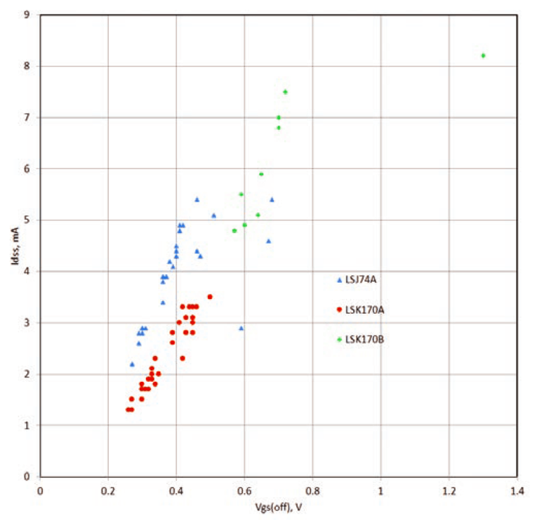
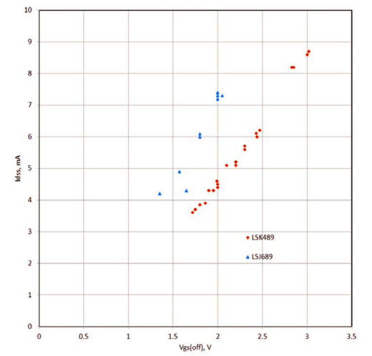
I measured the distribution of the JFET drain saturation current IDSS as a function of pinch-off voltage Vp for different samples of the LSK170A, the LSK170B, the LSJ74A, the LSK489, and the LSJ689. I measured about 50 samples of each single device and about 10 samples of each dual device. (Excel spreadsheets with additional data are available in the Supplementary Materials section of the audioXpress website.) Next, I performed the measurements with the MCubed Electronix semiconductor analyzer.
Measurement results are shown in Figure 1 for single devices and in Figure 2 for dual devices. Each dot on these graphs represents a particular device. Dots do not fall on a single line because of the variation in the JFET manufacturing process. It looks as though the LSJ74A devices have wider spread of IDSS than the LSK170A devices, but the LSJ74A with higher IDSS can be paired with the LSK170B.
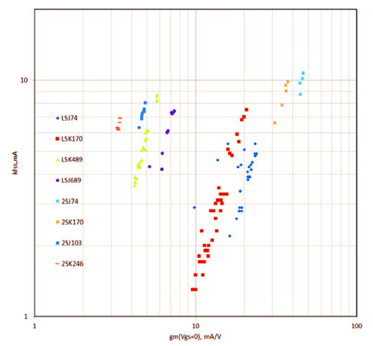
The data shown in Figure 1 and Figure 2 were used to calculate transconductance at VGS = 0. Drain saturation current IDSS as a function of transconductance at VGS = 0 for selected Linear Systems and Toshiba JFETs is shown in Figure 3. It is clear that for each complementary pair, the P-channel JFET has higher transconductance then N-channel device at the same ID. IDSS matching for complementary devices does not always lead to equal transconductance and compensation of even harmonics.
Circuit Description
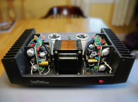
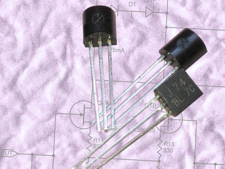
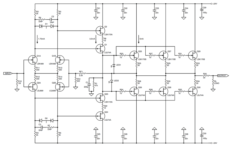
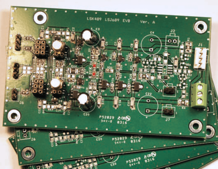
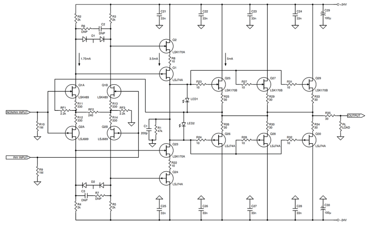
Figure 4 shows the all-FET amplifier schematic. Photo 1 shows the evaluation board. The circuit follows design principles outlined by John Curl and Erno Borbely for JFET amplifiers (see Resources). The input stage is a complementary differential circuit. The differential gain stage is realized with dual transistors Q1 and Q2. Each of these JFETs is working with 1.75mA drain current, which is set by source resistors R11–R14. Q1 and Q2 are dual monolithic JFETs, the LSK489 and the LSJ689 respectively. JFETs inside these pairs are matched closely thus input DC offset voltage of the all-JFET amplifier is low. Measured DC offset voltage is below 1mV. Such low offset allows omitting the DC servo circuit for certain applications. The second stage is the dual differential amplifier circuit (see T. Davis, W. Kulas, R. Lohman, and G. Sziklai patents in Resources).
Each differential amplifier has two JFETs of opposite polarity. The sources of the JFETs are connected with a resistor (R21 or R22). Drain of the first JFET (Q22 or Q23) is connected to the load R1 and drain of the second JFET (Q21 or Q24) is tied to the supply rail. The second stage couples to the input stage through drain resistors R2–R5. The second stage operating current value is slightly lower than IDSS and is about 3.5mA.
The open-loop gain is set by transconductance of the input and second stages and resistive loads for the input (R2-R5) and second stages (R1). With R1 = 47kΩ, the open-loop gain is 63dB. Open-loop frequency is set by capacitive load (C2 and input capacitance of the output stage) of the second stage. With 200pF the bandwidth of a closed-loop is around 15kHz. The amplifier is stable with the closed-loop gain above five. For the lower closed-loop gain series, RC network (C2, R6 and C3, R7) should be inserted between input stage drain resistors (R2, R3 and R4, R5).
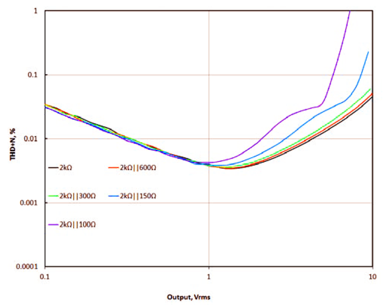
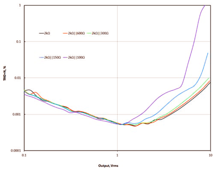
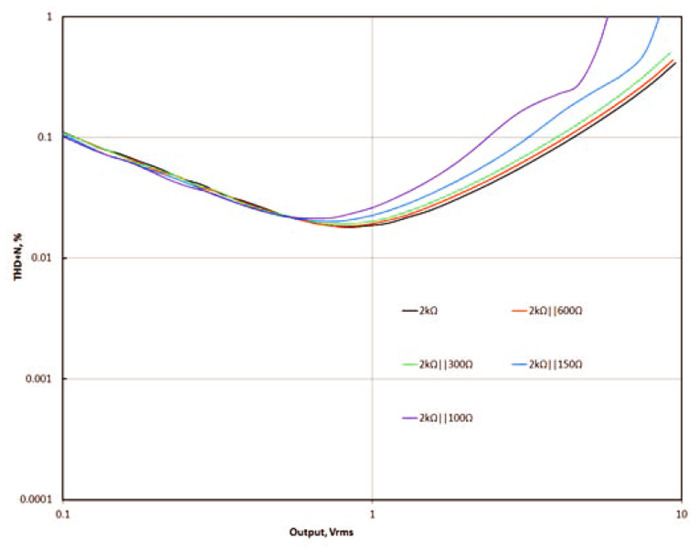
The second stage output is buffered from the amplifier load with a complementary source follower stage constructed with transistors Q25–Q30. Each output device operates slightly below IDSS with the drain current close to 5mA. The total bias current is 15mA and the output stage works in Class-A with light loads (above 600Ω). The amplifier can drive loads down to 150Ω, with no increase in total harmonic distortion (THD). Source resistors in the output stage are carefully selected to prevent distortion increase while switching from Class-A to Class-B operation with heavier loads. Each output device has a large copper pad for better heat dissipation. Light emitting diodes (LED1 and LED2) limit the voltage on the gates of output devices, thus limit the output current, and provide output short circuit protection. The current limit is about 85mA, and the amplifier can drive 100Ω load with up to 6 VRMS. Small resistors are included in series with gate of each output JFET to suppress any potential parasitic oscillation in the output stage.
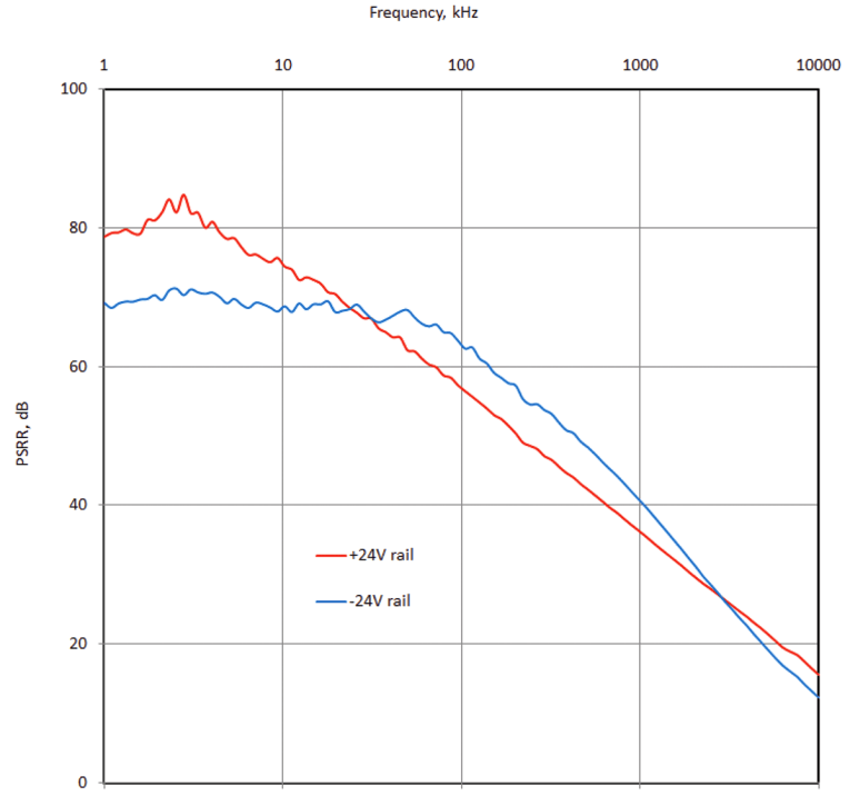
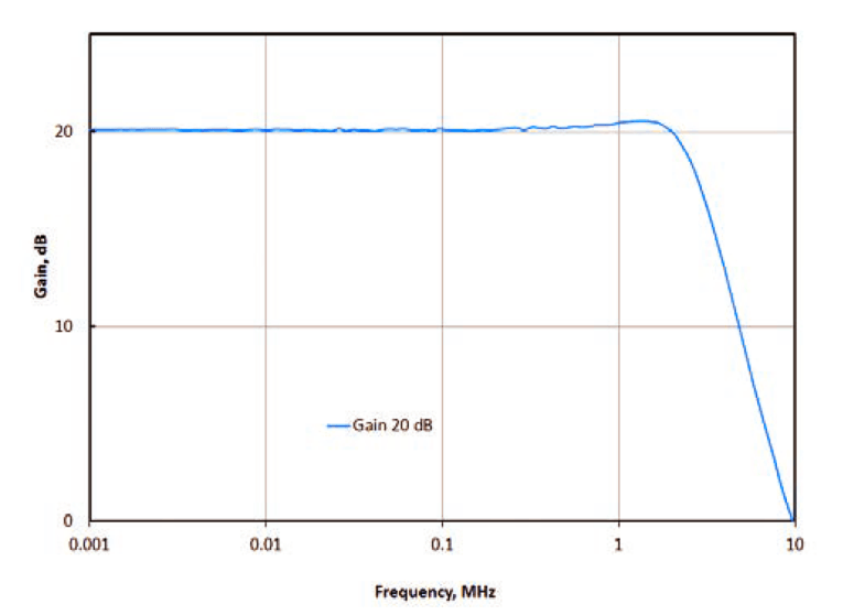
The closed-loop amplifier bandwidth (closed-loop gain is equal to 20dB) is wider than 2MHz. Frequency response and distortion for different gain setting will be discussed later in detail. The circuit shows good power supply rejection. Power supply rejection ratio (PSRR) is about 60dB at 100kHz. Figure 5 shows the plot PSRR vs. frequency for the all-JFET amplifier.
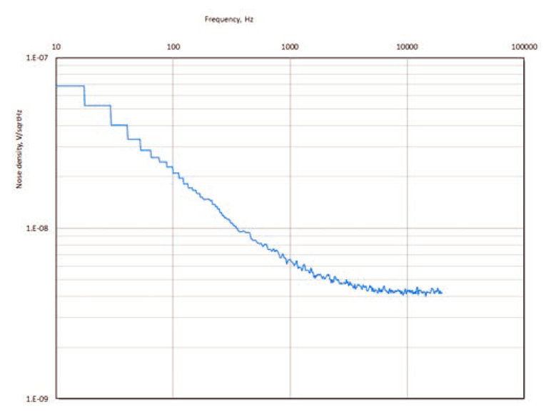
The circuit also shows good noise performance. Equivalent input noise in 10Hz to 22kHz frequency range is 0.7μV or -123dBV. The noise is 123dB below a reference point of 1V (0dBV). Figure 6 shows the amplifier’s input voltage noise density. Voltage noise density for source resistors R11–R14 is 2.3nV/√Hz. The total noise density for a single LSK489 with 330Ω source resistor is:

Measured input voltage noise density at high frequency is 4nV/√Hz. Measured noise is higher than calculated. The input stage has low gain (about 6 dB) and thermal noise of drain resistors (R2–R5) makes significant contribution to the amplifier’s total noise. The noise can be reduced by implementing active loads, reducing value of source resistors (R11–R14), by paralleling several JFETs and by using LSK389 with a future dual monolithic 1nV/√Hz low noise, high-transconductance P-channel device.

Amplifier Performance for Gain of 10
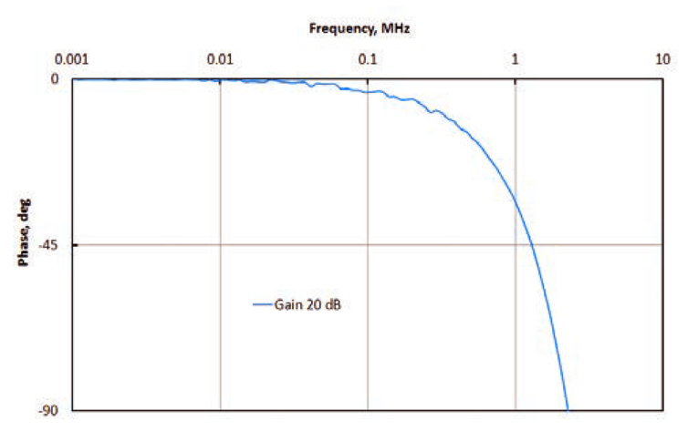
Figure 7a and 7b shows the closed-loop frequency and phase response for all-JFET amplifier. Figure 8 shows THD at 10 kHz plus noise for different load as function of frequency. The distortion profile is consistent for different loads. Distortion for 100Ω load increases for the output above 6 VRMS. This sharp rise is caused by current limiting action of LED1 and LED2.
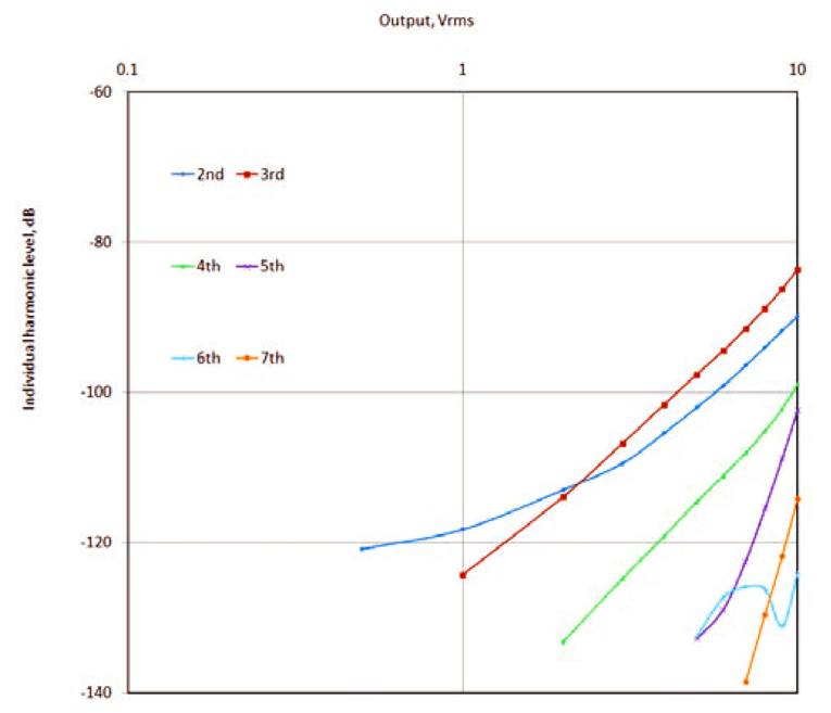
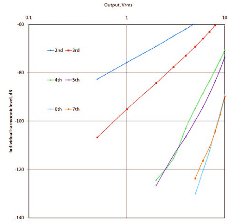
Figure 9 shows the harmonic distortion spectrum. It looks as if, with audio reproduction, the quality of the harmonic distortion is important with respect to its quantity and different subjective sonic results correlate with different individual harmonic distortion profiles (see Jean Hiraga’s article in Resources). The optimum harmonic distribution is characterized by a progressive decreasing harmonic distribution pattern with the absence of higher-order products. In this amplifier level of higher-order harmonics (fourth, fifth, sixth, and seventh) is at least 20dB below than the level of the second and third. The second harmonic is prominent at low and moderate output level (below 7 VRMS). The third harmonic prevails slightly at higher output level.
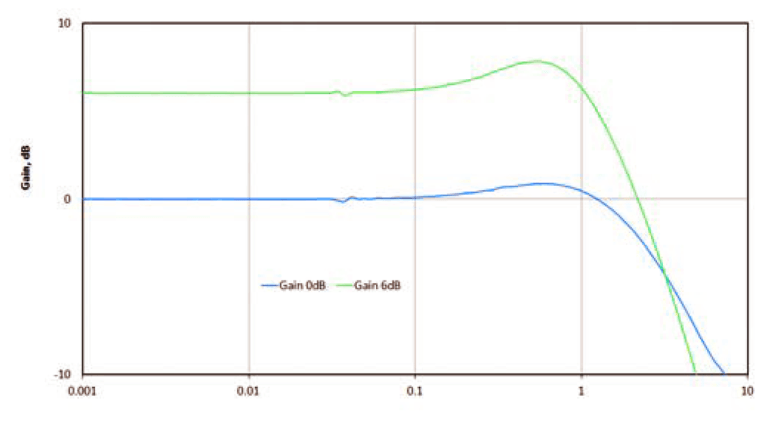
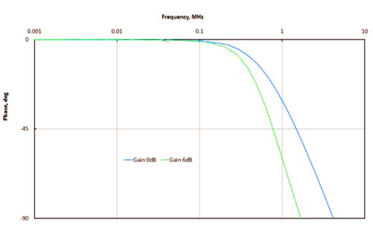
Amplifier Performance for Gain of 2 (6dB) and Unity Gain (0dB) Figure 10a and 10b shows closed loop frequency responses for the all-JFET amplifier. Figure 11 shows THD at 10kHz plus noise for different load as function of frequency. THD is under 0.01%. Figure 12 shows the harmonic distortion spectrum. Extra 20 dB of loop gain pushes all the harmonics down. There is still considerable gap (about 12dB) between the second, the third, and higher order harmonics. Lower order harmonics (second and third) behave in the same way as for amplifier with 20dB gain.
Importance of the Signal Source Impedance
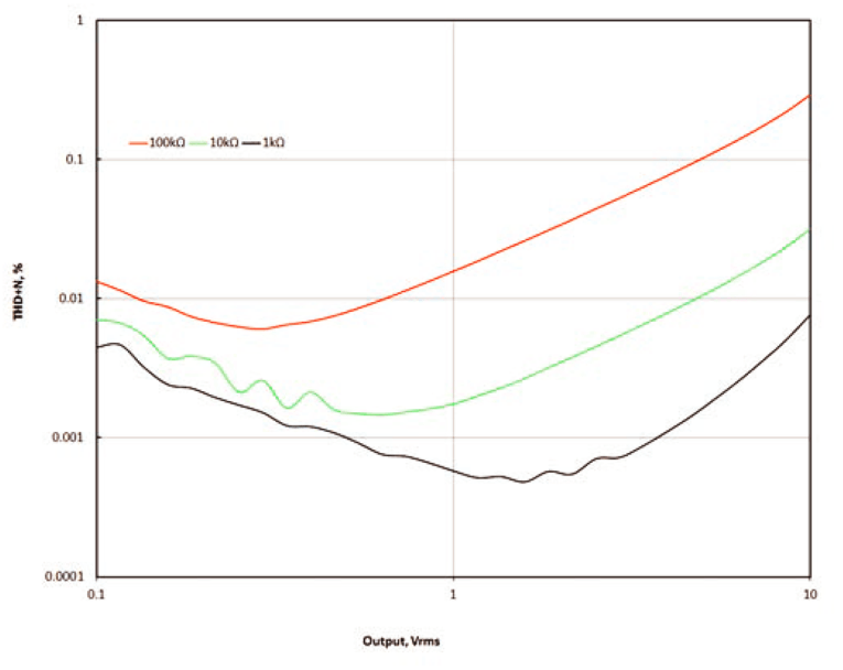
The LSK489 and the LSJ689 dual JFETs have small gate source (~4 pF) and gate drain capacitance (~1.5pF). The frequency response of an all-JFET amplifier with unity gain and a signal source resistance of 100 k has high-frequency rolloff with a -3dB frequency about of 200kHz. The input capacitance of the all-JFET amplifier with unity gain is about 8 pF.
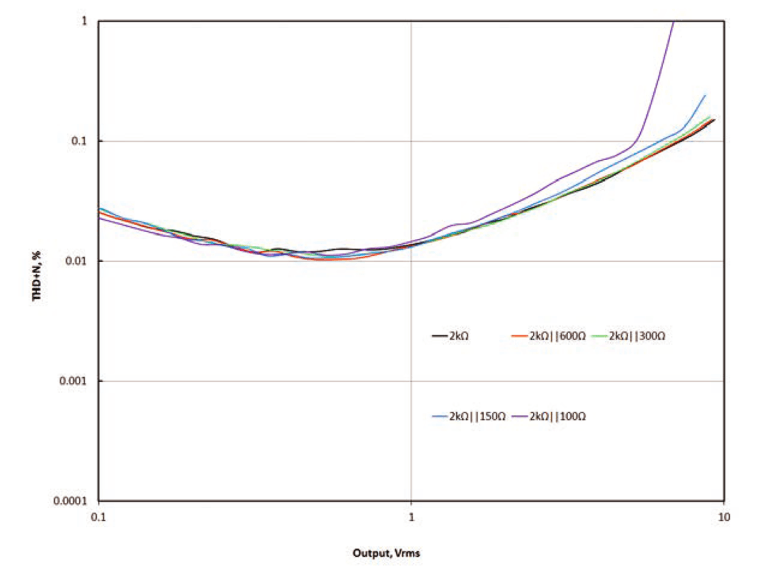
Figure 13 shows the total harmonic distortion plus noise (THD+N) as a function of output amplitude for gain x1 (0dB) and different source resistance (1k, 10k, and 100k. One can observe the distortion rise even when the source impedance is equal to 10k. In the "LSK489 Application Note," Bob Cordell suggested that a lower-capacitance device can help to create a circuit that is much less susceptible to intermodulation distortion with higher source resistance. However, the input capacitance of the JFETs is voltage dependent, and even being low, when driven from high impedance it can cause distortion, as shown in Figure 1. If extremely low distortion is required with higher source resistance and large excursion of the input signal, it may be obtained by cascoding of the input JFET with another JFET or with bipolar transistor (refer to Erno Borbley and John Curl articles in Resources).
Figure 14 shows the measurements of the level of each harmonic. It is generally accepted that reverse transfer capacitance of JFET is strongly nonlinear and cause high order distortion products. While one can observe increase in higher order distortion, second and third harmonics are prevailed with a considerable margin. This is due the fact that the junction capacitance varies inversely as a square or cube root of applied reverse voltage, depending on doping profile.
Balanced All-JFET Amp with Current Mode Feedback
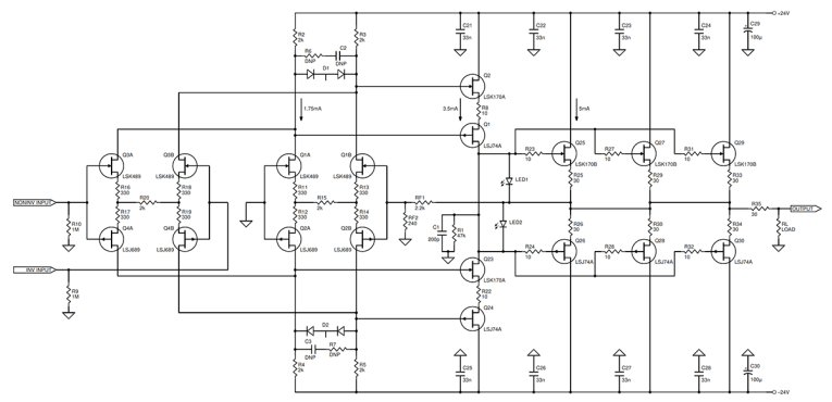
An amplifier with balanced input responds only to the potential difference between its two terminals—inverting and non-inverting inputs. Balanced input may be preferable because it rejects ground loop-induced noise and suppresses the interference from the environment. There are many realizations of balanced inputs — with transformer, differential amplifiers, etc. Figure 15 shows a different solution (refer to D. F. Bowers and R. Demrow articles in Resources). All-JFET amplifier employs current mode feedback (Resistors Rf1–Rf3) to the input JFET sources.
Figure 16 shows the measurements results for this circuit for 20dB of gain. Distortion is 6 to 10dB higher than distortion in non-inverting amplifier with single-ended input. Resistor Rf2 between the sources reduces the input stage transconductance and the open loop gain. Additional distortion is caused by asymmetry of the feedback network Rf1–Rf3.
Balanced All-JFET Amp with Current Summing
Figure 17 shows a balanced All-JFET amplifier with current summing (refer to the A. P. Brokaw and P. M. Timko article in Resources). Q3 and Q4, and R16–R20 form the first transconductance stage, and the second transconductance stage consists of Q1, Q2, and R11–R15. Drains of the transconductance stages are cross coupled so that the currents are subtracted and the result is fed back in the correct polarity. Input transconductance stage works without global feedback, and to obtain low closed-loop distortion both transconductance stages should have identical transfer characteristics. Resistors R15 and R20 provide local feedback in transconductance stages making their transfer less dependent on JFET pairs matching.
Figure 18 shows the measurements results for this circuit for 20dB of gain. One can observe elevated noise level, caused by local feedback resistors (R15, R20) in the transconductance stages. The overall gain is set by Rf1, Rf2 and the transconductance ratio of both transconductance stages. To improve overall distortion one can use dual parts in such way that first transistor in the pair belongs to first transconductance stage and the second transistor belongs to the second transconductance stage (opposite to the figure shown in Figure 17). This may cause DC shift, which can be removed by a servo circuit.
It might be worthwhile to combine a JFET input pair, which can be optimized for a specific source (e.g., a magnetic cartridge) and a BJT feedback pair. Another interesting application is differential current to voltage converter. In this case, current (e.g., from DAC) can be injected in the source network of the input pair.
Summary
This is an All-JFET amplifier. Measurements have shown that amplifier harmonic pattern remains unchanged with the output load. It appears that the distribution of harmonics with output level match to the pattern that was produced by the ear. This may provide a certain auditory benefit. aX
This article was originally published in audioXpress, October 2017
Project Files
To download additional material, visit the Supplementary Material page.
Resources
E. Borbely, "Starter Kits: EB-604/410 All-JFET Line Amp," audioXpress, March 2005. Available online
———, “Starter Kits Series: All-JFET MM/MC Phono Preamp: Part 1,” audioXpress, June 2005.
———, “Starter Kits Series: All-JFET MM/MC Phono Preamp: Part 2,” audioXpress, July 2005.
D. F. Bowers, “An Ultra-Low-Noise Monolithic Microphone Preamplifier,” Convention Paper
No. 2495, 83rd Audio Engineering Society (AES) Convention, October 1987.
A. P. Brokaw and P. M. Timko, “An Improved Monolithic Instrumentation Amplifier,” Institute of Electrical and Electronics Engineers (IEEE) Journal Solid-State Circuits, Vol. SC-10, No. 6, December 1975.
B. Cordell, “LSK489 Application Note”, Application note,
www.linearsystems.com/assets/media/application_notes/LSK489_Application_Note.pdf
J. Curl, “JC-2 Preamplifier,” The Audio Amateur, No. 3 1977
———, “JC-3 Power Amplifier,” The Audio Amateur, No. 2 1981.
T. Davis, “Differential amplifier circuits,” US Patent 3815038 A.
R. Demrow, “Evolution from Operational Amplifier to Data Amplifier” Analog Devices, Application Note, 09/1968,
www.analog.com/en/education/education-library/evolution-opamp-to-data-amplifier.html
J. Hiraga, “Amplifier Musicality,” Hi-Fi News & Record Review, March 1977.
W. Kulas, “Wide band transistor amplifiers with reduction in number of amplifying stages at higher frequencies,” US Patent 3562659 A. R. Lohman and G. Sziklai, “Emitter coupled transistor amplifier,” US Patent 2885495A.
 About the Author
Dimitri Danyuk has been the principal hardware engineer at Harman Luxury Audio division since 2013. He graduated with honors from Kyiv Polytehnic in 1985. His passion is to help audiophiles in all aspects of audio design. His articles have appeared in a number of magazines including the Journal of the Audio Engineering Society, IEEE Transactions, EDN, Electronic Design, etc. Danyuk also provides consulting services for various businesses.