In a philosophical sense, there are different levels of technology — most commonly, we think of fundamental and applied technologies. An example of the former would be the invention of transistors at Bell Labs in the 1940s. The driving force behind the fundamental advance was telecommunications, a much wider market than audio, but the availability of devices using the new technology transformed the consumer electronics markets. Once the concept of controlling electron flow in a semiconductor was established, it was a matter of application to use this technology in places such as audio, and over the years, audio-specific devices were created based on the fundamental telecom technologies. Audio was not the driver of technological change, but was the lucky recipient of its benefits.
Analogously, integrated circuits (ICs), computer networking, optoelectronics, lasers, micromechanical devices, and nanotechnology were not created for audio, but had a rapid uptake once they were commercially available because of the huge advantages in performance, efficiency, and reliability. Of course these days, there’s no shortage of audio use of exotic materials, such as graphene, carbon nanotubes, and the like.
While some technological adoption has been more for buzzword and gimmick value, gallium nitride (GaN) semiconductor devices are the real deal and have great promise for real performance gains in consumer and professional audio. In this article, I’ll briefly review what GaN is all about, why it’s important in general and to audio specifically, and discuss a couple of real-world examples.
GaN In a Nutshell
GaN is a wide bandgap semiconductor (3.4eV compared to 1.1eV for silicon and 0.67eV for germanium) originally used in optoelectronics—its wide bandgap means that the photons emitted are high energy, and thus short wavelength. GaN’s adoption (as with the similar gallium arsenide) was key to achieving efficient blue LEDs. A major difference from silicon is that the gallium-nitrogen bond is polar, and structures can be formed with one dimension (parallel to the Ga-N bond) being very different than the other two. The wider bandgap means that GaN devices can have higher breakdown voltages and withstand higher operating temperatures as well. Additionally, GaN is a direct bandgap semiconductor, that is, one where the top of the valence band and the bottom of the conduction band have the same momentum. This is key to its utility in optoelectronics, because promotion of electrons from valence to conduction bands only requires absorption of a photon of energy equal to or greater than the bandgap instead of needing the photons to interact with lattice phonons, as is the case for indirect bandgap semiconductors.
The unique structure of GaN crystals allows the creation of thin layers having exceptionally high electron mobility, defined as the ratio of electron velocity to applied field. So high-mobility electrons can be accelerated to high velocity, which implies high attainable device speed and efficiency. Because the electrons are constrained to a very thin layer in the vertical direction but have high mobility in the two horizontal directions, the electrons act as though they were particles in a gas (i.e., almost entirely free to move with low scattering). Thus, this layer is called a “two-dimensional electron gas,” or 2DEG. This 2DEG is key to the efficiency and speed performance of GaN devices.
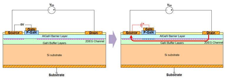
So we effectively have a sheet of highly mobile electrons. The conductivity needs to be switchable, in the manner of a gate in a conventional MOSFET, so a depletion region is created. A gate electrode is then used to increase electron mobility and density in that region for device turn-on. Compared to silicon, GaN is a more expensive material, and requires different (read: high investment) capital equipment for device fabrication. To overcome this issue, manufacturers developed processes to allow GaN fabrication on a silicon substrate. A typical construction for such a GaN High-Electron-Mobility Transistor (HEMT) is shown in Figure 1. The gate can either be isolated, with field used to turn on the conductivity, or fabricated as a heterojunction, with differing band-gaps used to create depletion under zero gate voltage conditions.
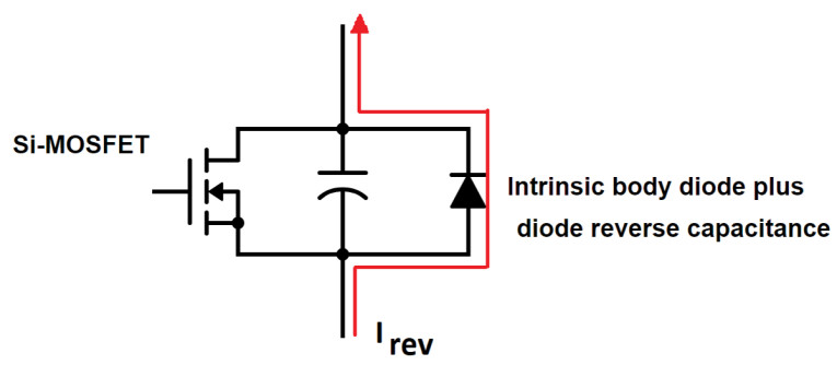
Besides increased electron mobility, there are several other advantages for GaN HEMTs’ speed. First, the gate resistance itself is quite low since the electrodes can be fabricated from metal rather than, for example, silicon nitride. Second, the gate threshold voltage (Vth) is significantly lower (roughly half or less) than that of silicon-based MOSFETs. For GaN Systems’ devices, the Vth is about 1.5V, with full turn-on by 5V Vgs. Third, unlike conventional MOSFETs, there is no intrinsic body diode. This means that the reverse recovery charge is vastly reduced to near zero. Putting numbers on that, QRR for a silicon MOSFET will be somewhere north of 1000nC and vary with charge/discharge rate, whereas a GaN Systems HEMT will have a QOSS of typically 60nC. These translate to faster and cleaner switching, which allows the reduction in deadtime and consequent reduction in distortion.
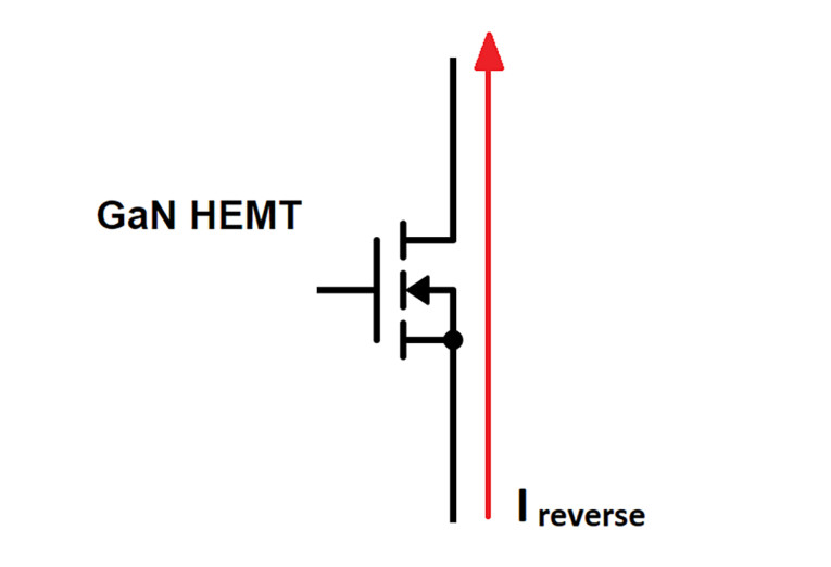
The fundamental operation and structure of the GaN HEMT allows reverse conduction through the body of the structure (Figure 2), in contrast to MOSFETs (Figure 3). This means an external diode path is also not needed, simplifying design. Because of the lower parasitic charges, the switching currents are also much cleaner, with far less ringing. This means that electromagnetic interference (EMI) suppression is much simpler.
The GaN Systems EVAL Boards
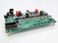
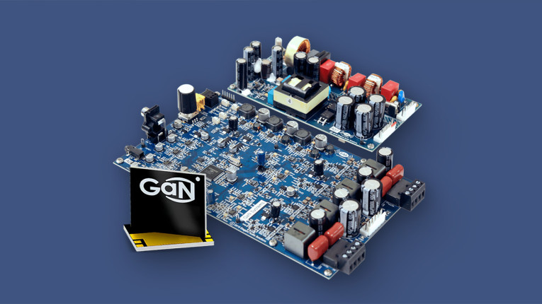
GaN Systems, a Canadian-based fabless semiconductor manufacturer, is one of the top suppliers of GaN power devices for automotive, power, and consumer electronics. To assist designers and OEMs in creating audio amplifiers using GaN technology, GaN Systems sells evaluation boards with a reference amplifier design and an accompanying power supply (Photo 1). These units were designed for GaN Systems by Skip Taylor at Elegant Audio Solutions (EAS), an Austin, TX-based design and engineering firm. Both the power supply and audio power amp circuits can be easily adapted for specific applications but are meant to highlight the preferred design practices to achieve a good trade-off between cost and performance, while optimizing the efficiency and cool-running advantages of their GaN devices.
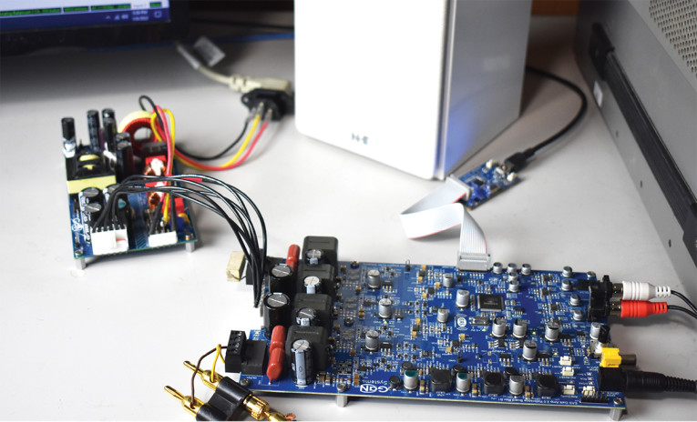
The GaN Systems reference design power supply is available with either a 12V DC input for designs targeted to automotive or 85V AC to 264V AC input for home audio. The supply outputs ±32V DC at up to 400W at efficiencies over 90% at full power out. It incorporates power factor control functionality as well, based on the NCP1654 PFC controller. The power circuit is configured as a half-bridge LLC resonant circuit, and both the PFC and power circuit use GaN System GS66506T 650V-rated HEMTs as power devices.
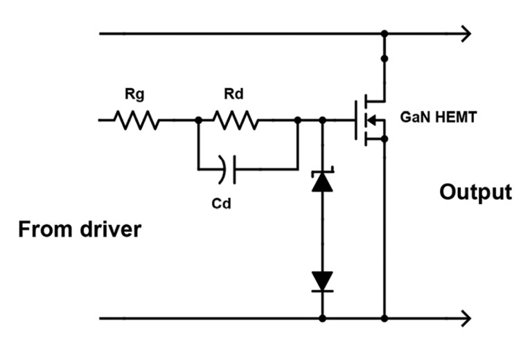
One interesting aspect of this supply is the use of a simple modification to the circuit driving the HEMTs. Since GaN HEMTs have different drive requirements (lower threshold voltage) than conventional MOSFETs, the designer has a choice between using controllers/drivers made for MOSFET circuits or controllers/drivers specifically made for GaN devices. The former choice is often made because of design features incorporated into the ”older” technology and lower costs because of the scale. In order to compatibilize a MOSFET driver with a GaN device, some GaN devices have drivers built in, which are in turn driven by the external MOSFET controller/driver. This of course adds cost and redundancy.
Instead, the GaN Systems power supply uses what they call an “EZ Drive,” which allows the use of a MOSFET controller/driver (e.g., an IRS2795), without having a second driver built into the GaN device. The EZ Drive circuit is remarkably simple and elegant (Figure 4), and consists of two resistors, a capacitor, and a Zener clamp.
The amplifier board itself is amazingly flexible. It has both analog (RCA and 3.5mm phone) and digital (SPDIF optical and coaxial) inputs, selectable by a push-button switch. There’s also a rotary optical encoder for volume control. The power stages use a full ground-referenced bridged output circuit driven by a pair of half-bridge controllers (TI LM5113) designed specifically for GaN circuits.
The output devices are GS61008P, which are rated at 100V and 90A. GaN Systems chose those devices instead of the 650V-rated HEMTs used in the power supply because of slightly easier drive and lower conduction losses. Output terminals are simple screw connectors. One interesting detail is the use of a Kelvin connection from the driver to the sources of the HEMTs, rather than connecting them all at the same point. This can result in a few decibels lower distortion, which is electrically significant when we get down to ultralow distortion levels. It’s a nice bit of attention to detail.
A very interesting feature of the GaN Systems EVAL board is the “open loop-closed loop” option, selectable by a push-button switch on the board. In the closed-loop mode, the audio signals from each side of the bridged outputs are fed into a differential amplifier, whose output is then used as a single-ended feedback signal to an earlier stage. In open-loop mode, that overall feedback loop is removed and gain re-adjusted in the signal flow. This provides a nice demonstration of the performance of the GaN output stage on its own.
Note that the open-loop mode only removes the overall feedback loop; local feedback around the op-amps used in the signal flow remains in place. I should also note that feedback is taken from the output HEMTs directly, before the output filter inductor, so the output inductor always stays outside the feedback loop. It has been claimed (see Resources) that this may have audible consequences, but to date, I am unaware of any rigorous double-blind comparison to support this.
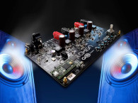
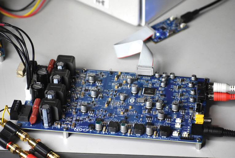
Before starting to fool around with the board’s capabilities, I hooked it up in my lab system for an afternoon, just to establish a baseline (Photo 2). I drove the EVAL board from the optical SPDIF input. In closed-loop mode, it sounded the same as the amp it replaced (which is good!). Switching to open loop, the gain actually dropped, which suggests something was going on in the audio processing beyond a simple loop-breaking. And once levels were matched, it did sound slightly different than the closed-loop mode on my reference amps. And different in a way that was familiar—one of my fun activities is designing and building tube amps, and darned if it didn’t sound just like one of them!
This got me looking at some basic performance attributes. For an uninteresting set of reasons, I was unable to use the Audio Precision source impedance utility, so I measured it manually by changing the load resistance and measuring the change in output voltage. From this, I could calculate the source impedance, which for the closed-loop mode was about 0.15Ω at 1kHz. In open-loop mode, the source impedance rose to nearly 1Ω. At 20kHz, the differences were even more significant, with closed loop measuring about 1Ω and open loop nearly 2.5Ω. These impedances will interact with a loudspeaker load (which varies greatly with frequency for most speakers) causing a frequency response difference. And that explains my subjective observation about the similarity to my tube amp. So, the open-loop mode can be an excellent way of dialing in the so-called “tube sound!” For the rest of my evaluation, I kept the amplifier in closed-loop mode.
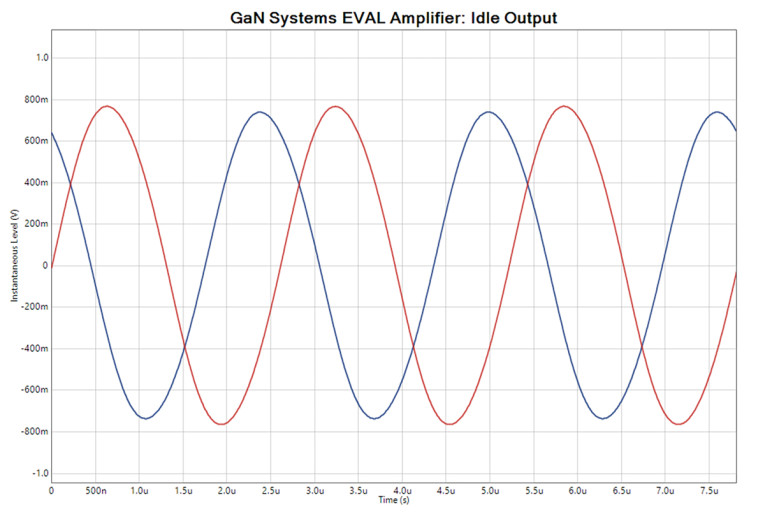
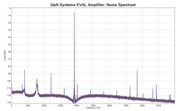
Putting the amp on my lab bench, I first looked at the output with no signal applied. The oscilloscope trace (Figure 5) shows that the oscillation frequency is on-spec at 384kHz. The level at the output terminals is about 500mV, which is par for amplifiers in this class, and absolutely insignificant with a speaker load. Interestingly, the signals for the two channels are roughly in quadrature rather than phase-locked. When asked about this, Skip Taylor of EAS responded that this is intentional and can help with reduction of EMI. I do not have the means to test this, but it seems plausible. The wide-band noise spectrum (Figure 6) confirms that the switching frequency dominates, with all other ultrasonic spikes below -85dBV. I asked about this choice of frequency, since GaN HEMTs are capable of switching at much higher frequencies than this. EAS responded that, in their experience, optimal performance is achieved at 400kHz or so, and that going faster brings no real-world benefit.
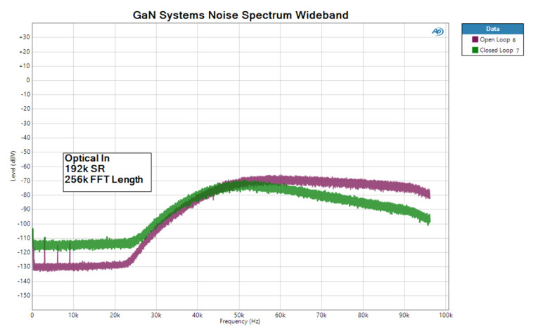
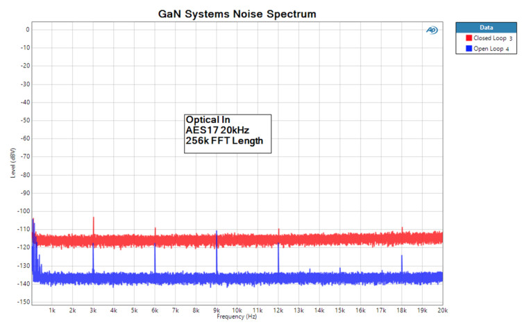
The feedback topology mentioned earlier has some interesting consequences regarding noise. Figure 7 shows the noise spectrum with no input in open- and closed-loop modes. In both cases, noise shaping pushes it out of the audible range and into the inaudible ultrasonic. But note that the open loop shows about a 15dB lower noise floor in the audible range (shown in more detail in Figure 8). This is likely due to the output noise of the differential amplifier in the feedback loop being amplified through the gain blocks preceding the driver chip. The closed-loop setting is by no means noisy, we’re talking about the difference between inaudible and really, really inaudible. Nonetheless, this is at least a theoretical and measurable advantage for open-loop operation under this particular feedback topology.
A quick check of power output showed that, with the power supply accompanying the EVAL board, clipping began at 150W into an 8R dummy load, both channels driven. Reducing the load to 4R, the amp’s power actually declined to 120W, suggesting that the limitation here is the power supply.
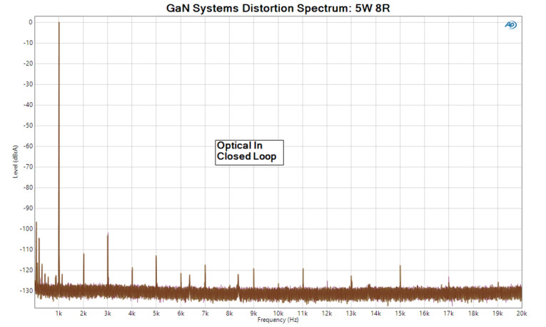
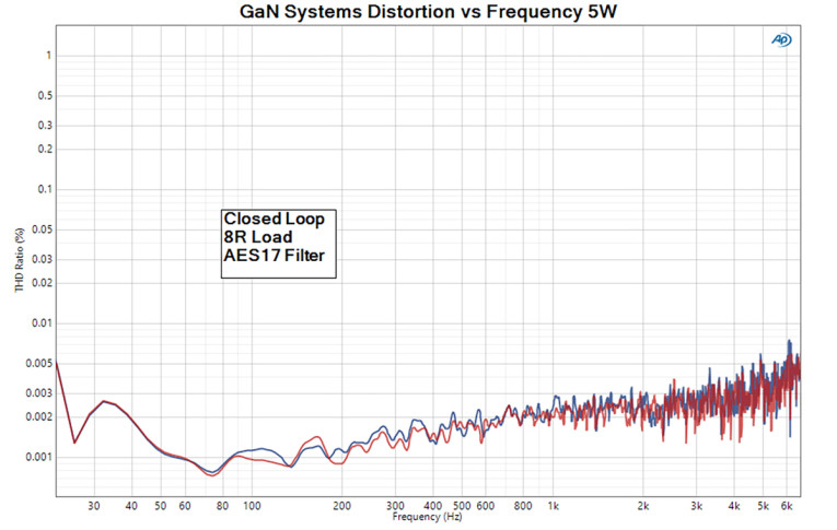
Figure 9 shows the distortion spectrum at 5W into an 8R dummy load. The dominant component is the third harmonic at less than -105dB down. This is excellent performance. Equally excellent is the relatively low frequency dependence of the distortion (Figure 10). Because of the AES17 filter, the measurements are only valid to slightly under 7kHz (the dominant third harmonic will exceed the measurement bandwidth), but the very slow rise with frequency is evident. It’s possible that even here, the dominant source could be noise, given the very low levels involved.
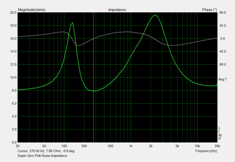
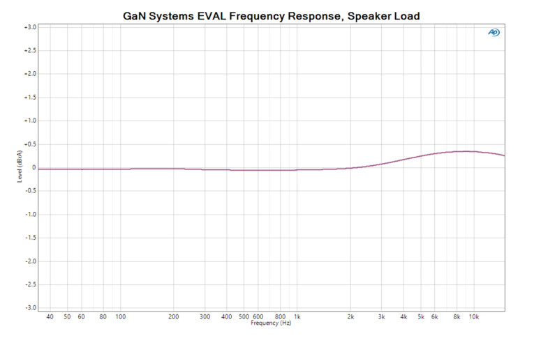
One question that arises again and again in discussions of amplification, and especially the newer Class-D technologies, is the effect of real-world speaker loads on performance. One of the speakers I regularly use is an old NHT two-way mini monitor. Its measured impedance is shown in Figure 11. I have used this impedance to create a reactive dummy load, but in my discussions with EAS, they felt that an actual speaker acted differently than a pile of coils, capacitors, and resistors. So I bit the bullet, plugged my ears, and ran some sweep measurements at 6.3V (corresponding to 5W into 8R). Figure 12 shows the frequency response of the EVAL into the actual physical speaker. The interaction between the output impedance and the reactive speaker load causes about a 0.25dB lift in the top two octaves. This might possibly be audible with direct rapid-switch ABX-style comparison and a pair of really sensitive ears, but is skirting human performance thresholds, so is unlikely to be a factor in real-world use.
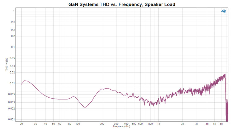
The distortion versus frequency sweep with the speaker load is shown in Figure 13. There are some peaks and dips correlating with the impedance changes in the speaker, but the distortion is still very low and generally flat. This is excellent performance for the intended application: driving loudspeakers.
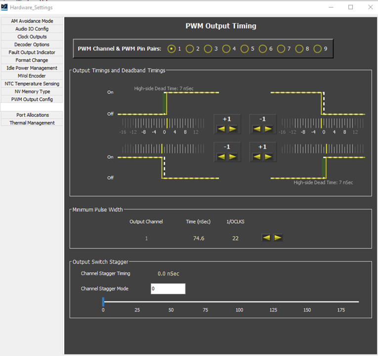
With the dongle attached and the drivers installed, you can choose the EVAL board as the target, then you will have access to hardware settings. Figure 14 shows one of the most important ones, pulse width modulation (PWM) timing. Here, you can adjust switching frequency, deadtime, and the interchannel delay in the switching waveform. These are parameters that will have a strong effect on distortion and efficiency — and they’re the easiest ones to set poorly and transmute the GaN into carbon. So this is a powerful tool, which must be handled carefully.
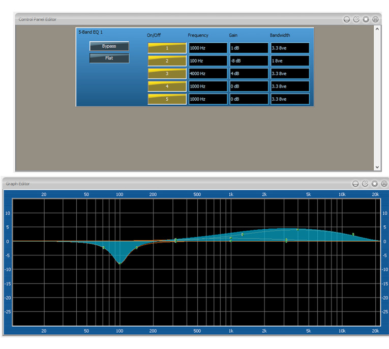
With the hardware settings finalized, the developer can start working with the audio signal flow. Figure 15 shows the default signal flow for the EVAL board, which the developer can modify. In this case, I added in a five-band equalization module to one channel by drag and drop using the software’s GUI. Figure 16 shows the particular EQ I implemented—it can be accomplished by entering values into a table or by directly tugging on handles on the frequency response graph. The software can be configured so that changes in the signal flow can be continuously sent to the amplifier so that their effects can be heard or measured in real-time.
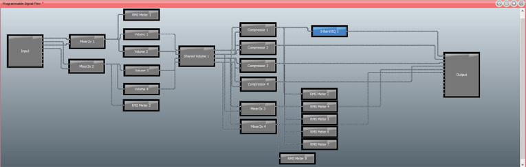
One note: The default signal flow is specific to the EVAL board. In the EVAL manual, EAS specifically warns about altering it (as opposed to adding functions). I, of course, knew better and proceeded to rework it the way I thought it should go. The dire warnings in the manual are more accurate than my self-assessment. Fortunately, Skip Taylor — my support contact indicated by GaN Systems — patiently walked me through reversing my errors and getting me back to a functional Square One. Moral: Believe the documentation.
Conclusions
I want to start this section out with a brief comment on the “Dog That Didn’t Bark.” The market drivers for GaN technology are electric vehicles and chargers, where the improved efficiency of GaN is a compelling advantage. These are applications where high power draw is the major use case. However, audio is different in that most of the time, the output power is relatively low.
Let’s take an example where Amplifier A runs at 85% output stage efficiency and Amplifier B runs at 95% output stage efficiency. So if it takes, say, 5W to keep the lights on (figuratively), at 1W of audio power, the total dissipated power by Amplifier A is 5.15W, whereas B will dissipate 5.05W. This is not a particularly significant difference.
Where we will see efficiency gains will be at high powers. For example, at 100W, Amplifier A will dissipate 20W, Amplifier B will dissipate 10W. That’s a lot more significant. But that’s also not common usage, and will in most cases not reflect the actual power used. So typically, the touted efficiency advantages, while real, won’t be huge overall.
That said, the GaN devices run cool, calm, and collected. The EVAL board has just about any features and programmability that a developer could want. As a reference design, it can provide an excellent starting point for new audio power amp designs. In my next article, I will show an example of this which has close to state-of-the-art performance in a tiny, light package.
In theory, you could put this board in a box, run a few wires, and you’d have a fully featured high-performance integrated amplifier. Or use it to develop (or be built into) active loudspeakers using the DSP features. Or voiced instrument or PA amplifiers. The open-loop mode sounds remarkably like a good quality tube amp.
The intersection between excellent engineering and a remarkable device technology is not inexpensive ($1265), but delivers great performance, flexibility, and value for the price.
UPDATE: Prior to press time, GaN Systems announced the release of a Gen 2 version of this evaluation kit, which features a reduced footprint power supply and enhanced protection circuitry for the audio board. The company also claims a further increase in efficiency and thermal performance. GaN Systems, also debuted a new groundbreaking GaN-based 500W Class-D audio amplifier reference that merges GaN power transistors and Class-D controller technology from Dutch company Axign (implementing a digital control loop with feedback behind the output filter, across the loudspeaker terminals), enabling new interesting possibilities that audioXpress looks forward to evaluating.
Resources
GaN Systems EVAL Board Manual, https://gansystems.com/wp-content/uploads/2020/05/GS-EVB-AUD-xxx1-GS_Technical-Manual_Rev-200526.pdf
GaN in Class D Audio, https://gansystems.com/class-d-audio-transistor-comparison
“An Introduction to GaN Enhancement-Mode HEMTs,” GaN Systems, July 2021,
https://gansystems.com/wp-content/uploads/2021/07/GN001_An-Introduction-to-GaN-E-HEMTs-210720.pdf
B. Putzeys, “This Thing We Have About Hysteresis Distortion,” Purifi Audio,
https://purifi-audio.com/2020/04/28/dist
“D2-3(S) Audio SOC Intelligent Digital Amplifier and Sound Processor,” Renesas Electronics D2Audio Datasheet, Renesas, April 2019,
www.renesas.com/us/en/document/dst/d2-926xx-d2-3s-audio-soc-datasheet?r=502821
This article was originally published in audioXpress, April 2022.