 Every audiophile understands the concept of the “sweet spot,” that happy balance of conditions that elicits the best possible sound. It can be a particular listening spot, the best positioning of loudspeakers, or the fortuitous combination of components which complement each other perfectly.
It should be no surprise that the desire for the best performance takes the search for the sweet spot into the interiors of the components themselves. This article will concern itself with finding the sweet spot for each gain device in audio amplifiers. It is a commonly held belief in audio that the best amplifiers are composed of one or more active gain stages, each made as intrinsically linear as possible before negative feedback is applied to further improve performance.
Taken to the extreme, linear stage = good / negative feedback = bad. The latter half of that statement is the subject of controversy, but there is no argument about linear stages being good. Achieving intrinsically low distortion in active devices (tubes or transistors) is usually not easy. You can use good parts, see to it that they have adequate voltage and current available, and use them in topologies that play to their strengths. These are the basics, and this is what you generally see when you examine schematics of popular amplifiers.
However, each individual device has a sweet spot where its performance is the best—often dramatically better — and finding that sweet spot is a powerful technique for maximizing the performance. I am writing about this because after years of communicating with DIYers and many professionals, I have discovered that this is a poorly understood concept, and I have seen many circuits which have failed to take advantage of it.
For every gain device, there is a number which characterizes the amount of gain. When you talk about distortion, you are talking about the alteration of the amount of gain in the device as the conditions change. The gain of a tube or transistor is altered primarily by changes in voltage across the device, current through the device, and the temperature of the device. Changes in any of these conditions change the gain, and all gain changes produce distortion. More precisely, they are the distortion.
Of course, the concept of a sweet spot depends on having an idea of what constitutes the best performance. It could be that you want the lowest measured distortion, a particular mix or phase of harmonics in the distortion waveform, the greatest efficiency, greatest power, or simply the best subjective experience when you listen to it. The sweet spot is whatever you want—after all, you are the designer.
I Brake For Tutorials
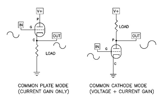
If you don’t mind a few basics, let’s look at examples of gain devices in generic circuits, starting with a triode (Fig. 1). This illustration shows simplified examples of the two most common gain stages using any kind of gain device, and the device pins are the Grid, Cathode, and Plate. In both cases the input signal appears at the Grid and variation of voltage between the Grid and Cathode causes a change in the current flow from the Plate to the Cathode. (All the examples you will see are simplified, and omit DC bias that may be present on the pins except for the V+ supply).
In Common-Cathode mode, the tube develops both current and voltage gain, and the output is taken off the plate, inverted in phase, and usually increased in amplitude. In Common-Plate mode, the tube seeks merely to have the Cathode voltage follow the Grid voltage, so the output voltage is ideally the same as the input, but with some current gain. That is why it’s called a follower.
For both modes you would normally look for the sweet spot—the conditions giving the best performance—by varying the values of the supply V+, the value of the load resistance, and the bias current through the device. Inevitably there will be some combination of these which is the best. Sometimes one of the circuit conditions is fixed; often it is the load value, in which case you vary the other conditions—the supply voltage and the bias.
In all of the examples later, I have chosen to simply look at Common-Plate (or Common-Drain/Common-Collector) performance, but the same ideas apply to Common-Cathode (or Source or Emitter) operation. Actually, Common-Drain circuits would seem to offer the least opportunity for improvement — as followers enjoying 100% degenerative feedback, they already have a much lower distortion character than Common-Source circuits. But you will see that even they can be improved, often dramatically, if you find the sweet spot.
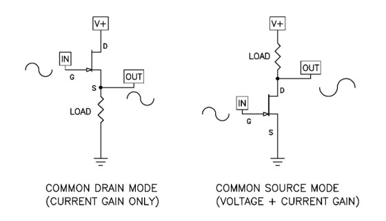
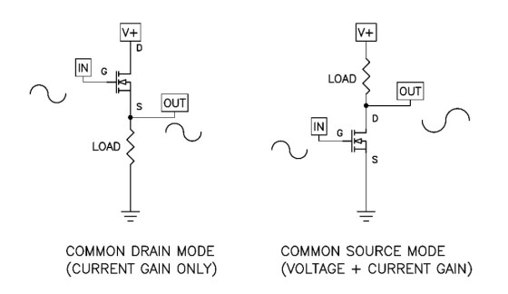
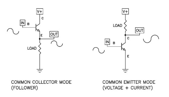
Figure 2 shows the example of the JFET counterparts to the tube circuits seen above. Here the pins are Gate, Source, and Drain. In the Common-Drain follower, the input voltage pretty much follows the output voltage, and in the Common-Source amplifier, the output is inverted and has both voltage and current gain available. Figure 3 shows the MOSFET example, which has the same pin designations as the JFET.
And last, Fig. 4 is the example of a bipolar transistor, where the pins are Base, Emitter, and Collector. The choice of a particular type of gain device—tube or transistor—is often arbitrary, but ideally it plays to the particular strength of the device for a given application. In principle you can substitute one type for another, but as a practical matter, there is usually a good reason for the selection of one over the others.
It doesn’t matter in terms of the idea of finding the sweet spot—the terrain changes a bit, but the game remains the same.
Getting To The Sweet Spot
For any of the above circuit types and devices, if you start with reasonable textbook values for the circuit, you will get reasonable performance. If you start to play with the values a little bit, you will find that the performance changes for better or worse.
Often you will find a combination of voltage and resistor values which give a lot better than the generic performance. That’s the sweet spot. If you have a distortion analyzer, you could simply run through the range of combinations of values and select the result you like best. If you simply want good measurements, you might be able to stop there. If you are looking for better subjective performance, you might find this a good place to start your listening. What creates the existence of the sweet spot in gain devices? To see where this comes from, look at the characteristics of some tubes and transistors.
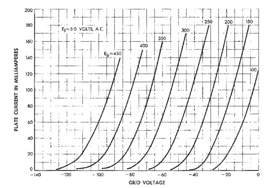
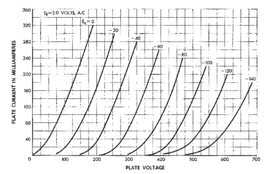
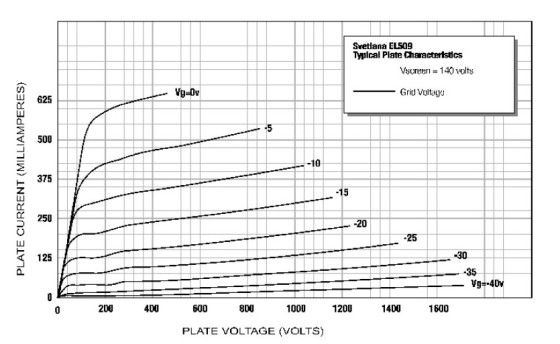
Let’s start with a simple big triode, the 300B. This curve (Fig. 5) shows the Plate-to-Cathode current as a function of Grid voltage, with each curve representing a fixed value of plate voltage. Looking at this figure, you see that the lines are curved — the more current, the faster they rise. Figure 6 is a different view of the same character, but with the current plotted as a function of the Plate voltage, with each line representing a fixed value for Grid voltage.
These lines are also curved with a shape very similar to the previous graph. A perfectly linear tube will have these lines in both graphs perfectly straight and equally spaced. Any deviation from that would be distortion. Looking at the curved lines, you can see that there is quite a bit of distortion.
For a given Plate voltage, the current increases exponentially with the Grid voltage, in what is known as a square law characteristic, resulting in second harmonic distortion. For a given Grid voltage, the current increases exponentially with the Plate voltage, also a square law and also creating second harmonic distortion.
In this curve the Y-axis is still the plate current, but the X-axis is now the Plate voltage, and each line represents the Grid voltage. It looks familiar—just as the plate current is an exponential function of Plate voltage, it is also an exponential function of the Grid voltage. This is a particularly important observation with respect to finding the sweet spot.

The Deal
Ordinarily in a tube amplifying an AC signal, a positive change in Grid voltage causes an increase in Plate current and is accompanied by a decrease in Plate voltage. The gain due to Plate current increases, and the gain due to Plate voltage decreases. The opposite happens when the Grid voltage goes negative. These two gain variations tend to cancel each other, resulting in more constant gain and lower distortion. If you choose your conditions so that the simultaneous gain increases and decreases are equal, you can lower the distortion a lot.
This technique is occasionally referred to as load-line cancellation. It is called that because the range of the device’s operation sits on a line in the transfer curve, and the particular shape and position of that line results in minimum distortion.
By some criteria, this would be the sweet spot. At this point you will probably find that your second harmonic has largely disappeared and you are left with some third harmonic. This is because you can’t completely cancel two square law distortions without leaving a cubic trace—the third harmonic. So, how much distortion reduction?
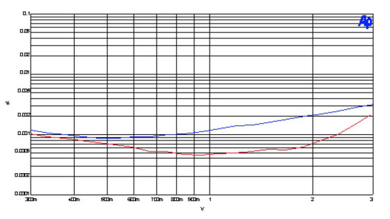
On a clear day, you can think in terms of a 90% reduction, as seen in the Fig. 7 curve, where a triode follower is operated at a high plate voltage giving the upper distortion curve. Without changing the load or the current, I simply reduced the Plate voltage until the gain dependence on Plate voltage matched the gain dependence on Plate current (as determined by lowest distortion at 1V) and ran the lower curve.
I think you can agree that this is a significant reduction, roughly equivalent to what you would see with 20dB of negative feedback, except that you have not attached a negative feedback loop and the output gain and impedance of the circuit remain about the same.
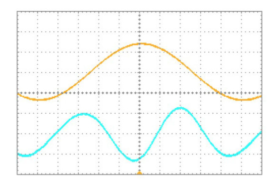
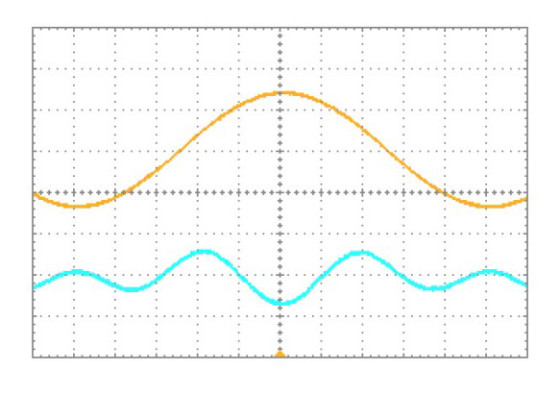
Because of the square law characteristics of the devices, the primary distortion is second harmonic in content, and when you cancel two second harmonics, you find that the remainder is a third harmonic. The original second harmonic looks like Fig. 8 on an oscilloscope viewing the output of a distortion analyzer. After cancellation, the harmonic content looks like Fig. 9. If your criterion instead is a particular harmonic content or harmonic phase, a deviation from this point in either direction will give you second harmonic back with its phase depending on which way you went, and you can tweak this in relation to the amplitude of the third harmonic if you like. There is a reason why triodes are popular in single ended applications — their gain dependence on Plate voltage is quite strong and makes for easy load-line cancellation.
This technique also applies to pentode tubes, although it will not be quite the same. The transfer curve of the pentode is much the same with regard to grid voltage, but the current variation due to Plate voltage is different. Figure 10 is the transfer curve of a pentode.
Here you see a family of curves which indicate that the gain (transconductance) increases exponentially with Plate current, but has less variation with respect to Plate voltage as compared to the triode. You can still vary the voltage, current, and load parameters to find the sweet spot, but it will be in a different place.
JFETs have the exponential current versus Gate voltage but enjoy a wider variety of transfer characters situated between triode and pentode and are generally well suited to exploit the concept of a sweet spot in single-ended Class A circuits.
You will note that these aren’t the tiny little signal JFETs that everyone is accustomed to. These are examples of the new generation of high-power JFETs coming out of the labs. In the 1970s, when Yamaha and Sony produced power JFET devices for use in their own amplifiers, it created some excitement among audiophiles. Unfortunately, it seems that they were ahead of their time, and now those parts are quite rare.
Fortunately, totally new devices show promise in modern power amplifiers, both as switches and linear amplifying parts—tomorrow’s transistors (at tomorrow’s prices). For power JFETs, the Ids dependence on Vds is partly a function of the Gate channel depth on the chip.
The pentode-like character is seen in high current power “Vertical” JFETs, and the triode-like character is seen in SITs (Static Induction Transistor). The enhancement mode power JFETs do well in single-ended Class A applications and can take advantage of loadline cancellation. My samples of depletion mode JFETs have a more pronounced voltage dependence, and are thus even more interesting.
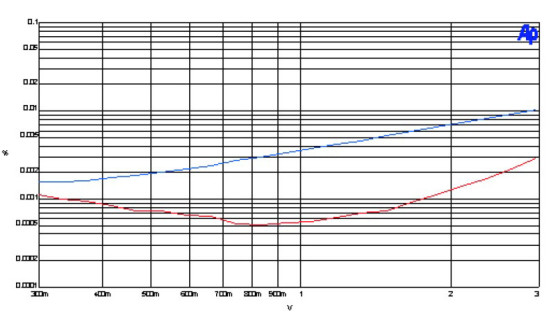
Figure 13 is an example of a JFET follower whose characteristic is mostly “pentode-like.” The upper curve reflects the distortion at V+ voltage near the device rating, and the lower curve shows the distortion cancellation available by searching for the “sweet spot” at a lower supply voltage. You can see that at 1V output, the distortion has been reduced by about 85%.
Alternatively, you could have adjusted the bias current or the load resistance, and also tried for best performance at some higher voltage than 1V out. This example was of one of those “little” JFET devices, but it works with parts of all sizes. You must remember that this cancellation is there somewhere, and you might want to go looking for it. Also keep in mind that the sweet spot is a bit different for every part, even within the same part types, and you will want to consider expending the effort for each individual part for the absolute in performance.
This is important when you change out tubes in an amplifier, as every tube-ophile knows they are all different. Setting them to a generic bias current does not guarantee the sweet spot for a given tube. You might want to consider how you can vary the supply voltage and the bias while evaluating the performance.
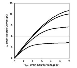
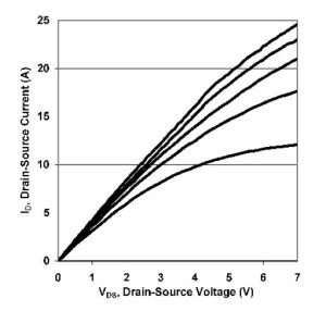
Figure 14 is an example of a power MOSFET’s transfer curve. Power MOSFETs have a character somewhat similar to a pentode. The Plate has been replaced by the Drain, the Grid has become the Gate, and the Cathode is now the Source.
You see from this diagram that the gain increases with Ids, but there is not a lot of dependence on Vds above a few volts. At just a couple of volts you operate in what is known as the “linear” region of the MOSFET, where there is strong dependence. You can work the load-line in this region effectively, but it is not a popular technique for a number of good practical reasons. Fortunately, for many MOSFETs operating in Class A, the distortion of the current transfer curve is low enough that you can still find the cancellation for a pentode type voltage characteristic—just go looking for it.
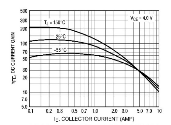
And, of course, someone is going to ask, “What about bipolar transistors?” It so happens that bipolars have a sweet spot also. Figure 15 is an example of the current gain figure of an ordinary NPN transistor versus Collector current. There is also a dependence on Vce known as the Early effect, a slight straight line dependency increasing with voltage. As with other devices, finding the sweet spot for a bipolar device means locating the point where these variations result in distortion cancellation.
In Fig. 16 you see the gain versus current curve of an NPN power transistor showing some gain dependence versus Collector current. Above a couple of volts, the variation is much less and forms a fairly linear straight line with voltage. Of course, you can work these two curves. The distortion curve in Fig. 17 shows a follower circuit like the others, but with a bipolar transistor. The upper trace is with a high supply voltage, and the lower trace is the reduced voltage. The reduction in distortion is less dramatic, but it’s still about 7 or 8dB better.