
The finished amplifier uses a very high-quality 800VA custom wound toroidal transformer running at about 25% lower flux density than normal commercial devices, and features a low noise stabilized core, an interwinding screen, and a GOSS band [11]. The twin secondaries (2 x 31.6V AC each at 4.5A load) are separately rectified and then each smoothed with 54,000µF, after which the two supplies are combined to create the split ±40V rails required by the amplifier.
An in-rush current limiter (Figure 6) and power controller (called the iSSDCB) [12] on the mains side prevents power-up surges, while a DC blocker circuit prevents transformer from “growling” in the event of a DC offset on the mains supply, a problem usually caused by appliances using half-wave rectification for crude power control (e.g., a hairdryer with a warm air setting). AC Hot and Neutral enter the board via AC Live In (U7) and AC Neutral In (U2). The neutral mains feed passes through C3~C6 (10,000µF 6.3V), arranged to AC bypass 45A bridge rectifier D4, which blocks mains DC offsets of up to of ±1.4V [13] with R2 and R3 (10k each) providing a discharge path. The full AC mains current load for 3000 hours at the 105°C rating of the paralleled bypass capacitors is 4.6A.

Without some form of limiting, peak in-rush currents will exceed 200A for the first 2~3 mains cycles. The neutral line feeds through to R1, a 10Ω or 20Ω Ametherm thermistor (value dependent upon the mains supply voltage), which on power up limits the peak current into the transformer primary to ~15A peak. About 2 seconds after applying power, the soft start relay (U6, 24V DC coil) engages, bypassing R1. U6 derives its power from C8 and C9 (330nF 250V AC-type X capacitors with parallel discharge resistor R4 at 220k) and a power on delay timer derived via R6 and R7 (220Ω each) and C7 (2200µF 35V). The neutral output from the soft start circuit appears at U8 (Neutral to TXFMR) from where it is routed to the power transformer.
The on/off power control is accomplished in the AC mains Live/Hot line from U7 using U1 (Power On/Off RL), also a 24V DC relay that similarly derives its power from a capacitor network (C1 and C2, 330nF 250V AC-type X capacitors and discharge resistor R8 220k), with C10 (100µF 35V) providing basic DC smoothing. When the amplifier is in the power-off state, the power switch connected across terminal U4 and U5 shorts out U1’s relay coil via R5 (220Ω), holding the relay and PWR ON LED off and via its associated contacts, blocking AC power to U3, the switched AC mains Live/Hot output (Hot to TXFMR). R5 is included in series with the switch to ensure the switch contact peak currents from C10 are limited to ~130mA.
When the power switch is opened, U1 coil is energized, the contacts close, and AC mains voltage appears at U3. Although this approach means there is a small standby power (approximately 0.2W) consumed by U1 when the amplifier is off, it allows the use of low current anti-vandal switches of which there are numerous attractive options. The worst-case voltage appearing across the switch connected across U4 and U5 is never more than 30V DC and the nominal DC current around 17mA. Note that for 120V AC operation, C2 and C9 must be mounted.
The power supply controller and DC blocker PCB is at mains potential and mains safety protocols and wiring standards must be strictly followed with this board.
Protection from DC offsets (including sustained hard clipping) and output short circuits is afforded by a UPC1237 IC-based module [14] that uses solid-state MOSFET switches to interface the amplifier to the speaker load. The circuit incorporates a 3~4 second delay before engaging the speakers, and very fast speaker turn-off on power down, ensuring there are no audible thumps from the speakers during power cycling.
Construction for Low Noise
Achieving the measured ax-Amplifier performance requires strict attention to PCB layout and design, cable routing between the input connectors, amplifier modules and the power supply; furthermore, the power supply PCB, chassis grounding, and transformer design and construction are also critical.
Both output halves conduct in Class A and there is considerable variation in the load current through the output stage devices resulting in radiating magnetic fields that can couple into the small-signal stages, causing distortion. On the ax-Amplifier PCB layout, the +, -, 0V, and output rails are all tightly coupled together with tracks either adjacent or overlaid on each other on the double-sided THP board. Additionally, the output NPN and PNP devices are interdigitated to further minimize radiating loop areas. In Class AB amplifiers, only one half of the output stage conducts at any one instant, so interdigitating like this is not strictly required to achieve lowest noise and distortion.
Peak reservoir capacitor charging current pulses exceed 12A in Class A and under sustained Class AB operation into 4Ω approach 20A, while on the primary side, the peak currents in Class A mode exceed 5A. For this reason, it is critical to ensure radiating loops are kept to an absolute minimum through good wiring practices. Like the amplifier module PCBs, the power supply board also has the +, -, and 0V traces overlaid to minimize radiating loops.
Figure 7 shows the physical amplifier wiring scheme, which must be strictly adhered to if the published specifications are to be met. The wiring to the front panel LED status indicator, overcurrent sensing to the speaker protection board, and the bias setting switch are not shown for clarity. Other than keeping them well away from the power supply and transformer, the routing of these is not critical for noise performance.

The power supply wires (red) consisting of V-, 0V, and V+, must be tightly bundled or plaited and cable tied to reduce the cabling loop area, as must the speaker wires to the speaker protection board (teal) and then from the speaker protection board to the speaker terminals (Photo 4).

The short thick green cable attached to the point marked “Safety Ground” on the PSU board uses one of the hex brass stand-offs to make a connection to the chassis. Use serrated washers and a closed ring terminal (do not use a “U” terminal as these can come loose) to make a good connection to the chassis and ensure every part of the chassis (cover plates, front and rear plate, heatsinks) is solidly connected to safety ground using an Ohmmeter. Use a good quality switched, fused IEC receptacle to bring power into the amplifier.
The amplifier accepts balanced inputs only directly through standard XLR connectors. It is recommended that pin 1 of the connector is connected directly to the chassis at the point of entry. In the author’s implementation, the XLR receptacle (Neutrik Part # NC3FAH1-D) securing screws are directly connected to pin 1 mechanically and accomplish this. It is important that the XLR screen is well connected to the source chassis and the ax-Amplifier chassis as this makes the entire system a single enclosure as far as RF is concerned.
Referring to Figure 8, the speaker return is routed from the output connector back to the amplifier module, and not directly back to the power supply 0V as shown on the left-hand side. If the speaker return is wired directly back to the PSU 0V as depicted on the left and a separate 0V line runs to the amplifier module, any voltage drop appearing across the amplifier module 0V from A to B couples to the inverting input via Rg through common impedance coupling.
By routing the speaker return back to the amplifier module, the voltage drops across the module 0V feed are minimized due to the lower connection resistance, and the loop area bounded by all 0V returns and the feedback resistors is greatly reduced. There is a further benefit in that magnetic fields arising from the high current speaker return do not potentially couple to the input via the module 0V return wire. In the ax-Amplifier, a significant reduction in power supply hum artifacts and distortion results from using the wiring method shown on the right in Figure 9.


Initial testing and setup are detailed in the Supplementary Material section of the audioXpress website (see Project Files). Once the amplifier has been assembled and basic tests completed, it is recommended that the transformer be rotated back and forth through ±60 degrees to find the noise null point using a sound card or audio test set. In toroid transformers that do not employ a GOSS band, hum reductions of 8dB to 10dB are readily achievable, while those with a GOSS band can show reductions of 2dB to 3dB. Once the null point is found, the transformer should be secured in place.
It should be noted that the ax-Amplifier is not suitable for use with unbalanced input connections using balanced to unbalanced adaptor cables due to the way the input bandwidth limiting filter is arranged.
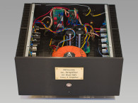
The amplifier was constructed in a diyAudio.com 5U Deluxe Dissipante pre-drilled chassis featuring its standard power device mounting configuration. Although large with substantial heatsinks, the finished amplifier heatsinks will run at close to 60°C under sustained Class A operation, so it is important to ensure it is located where there is good airflow and to this end, the amplifier feet are important in ensuring the chassis is at least 5cm above the floor. Photo 5 shows an image of the finished project.

Measurements
All the measurements shown were conducted on a completed amplifier and done with a QuantAsylum QA401 Audio Test System using all balanced interconnects. Figure 10 shows the system noise floor with the amplifier powered in Class A but with no input signal. The noise floor at 1kHz is approximately -135dB reference 60W into 8Ω. The peak mains noise component is -130dBr at 150Hz.


The amplifier performance in Class AB mode is shown in Figure 12. At 70W the distortion is 9ppm and the mains noise component at -128dBr. The output PSU related noise is 2dB better in Class AB because the PSU ripple is lower due to the lighter current draw.

In Figure 13, the right channel has AFEC disabled, and the amplifier is driving 2Ω delivering >200W into the load. On the AFEC-enabled left channel, the distortion is 12.5ppm and on the non-AFEC-enabled channel, 147ppm. AFEC has thus suppressed distortion at high powers by more than 20dB.

Figure 14 and Figure 15 show the amplifier’s performance into various capacitive loads, along with clipping performance.


Figure 16 shows the ax-Amplifier intermodulation distortion (IMD) performance with a 19+20kHz full power stimulus. The 1kHz intermodulation tone is at -118dBr. This is a significant improvement of 10dB over the system without AFEC and in Class AB mode without AFEC (-95 dBr), a 23dB improvement. The amplifier performance into 4Ω and 8Ω is plotted in Figure 17. The generator THD+N is specified at -108dBV, so is the larger contributor to overall distortion in this plot below the onset of clipping. Finally, in Figure 18, THD vs. frequency at 25W and 50W into 8Ω is shown. This data, in conjunction with the 19+20kHz IMD result attests to the ax-Amplifier’s good high-frequency linearity, which is a consequence of the wide loop gain bandwidth and high loop gains.


Summary and Conclusions
Achieving the performance demonstrated with this amplifier using conventional design approaches would require raising amplifier loop gain using an EF3 output stage, a more advanced TIS (e.g., a Hawksford VAS) and ripple eaters in the supply rails to the amplifier front end. With AFEC, this additional complexity and cost are dispensed with and in its simplest form, using just a single good quality op-amp, two precision resistors, and a low value COG/NPO capacitor, class leading performance is attainable. AFEC’s primary effectiveness is in dramatically reducing large signal TIS and output stage non-linearity and improving PSRR.
Previous work with this technique has shown it will help counter some of the deleterious effects of cross-over distortion in sub-optimally biased output stages. Another important benefit of AFEC is that the amplifier can deliver more peak power in the low distortion regime for given power supply voltages, where, without it, the distortion would be rising rapidly. The combination of greatly improved PSRR of up to 30 dB, distortion reduction across the audio band and at high power levels, along with ease of implementation make this an attractive technique. As with any feedback or feedforward technique, AFEC should not be used to ameliorate badly engineered power amplifiers, but rather to raise already well-designed and engineered amplifiers to class-leading SOTA performance.
Author’s Note: Readers wishing to build the ax-Amplifier can purchase PCBs at www.hifisonix.com. For US based builders, the ax-Amplifier housing is available at diyAudio.com and for European builders, directly from Modushop. aX
Project Files
To download additional material including initial testing and setup, visit:
http://audioxpress.com/page/audioXpress-Supplementary-Material.html
References
[9] “The Baxandall Papers,” www.douglas-self.com/ampins/baxandall/baxandall.htm
[10] B. Cordell, Designing Audio Power Amplifiers, 2011, pp. 177-183.
[11] Tiger Toroids Audio Transformers, www.tigertoroids.co.uk
[12] Improved Soft Start + DC Blocker iSSDCB Imroved Soft Start + DC Blocker aka iSSDCB | Hifisonix Projects, www.hifisonix.com
[13] R. Elliot, “Blocking Mains DC Offset From Transformers,” Elliott Sound Products, 2008, https://sound-au.com/articles/xfmr-dc.htm
[14] “Hifisonix Loudspeaker Protection Board,“ Hifisonix, https://hifisonix.com/projects/hifisonix-speaker-protection-board/
Click here to read the First Part of this article
This article was originally published in audioXpress, May 2024