
Augmented Feedback Error Correction (AFEC) is a technique wherein a high-performance small signal amplifier (here half of a dual OPA1642 op-amp) augments a power amplifier’s loop gain by up to +40dB. AFEC significantly suppresses power supply artifacts, lowers distortion by up to 20dB even at high output powers and maintains amplifier DC offsets near 0V. The power amplifier stage utilizes a current feedback amplifier (CFA), transitional Miller compensation (TMC), a double emitter follower (EF2) output stage, and accepts balanced inputs. The output stage standing current can be switched between Class A, Class AAB, or Class AB with an automatic bias control switch reverting the amplifier to Class AB when not playing music, reducing power consumption by up to 70% over Class A operation.
AFEC Operation
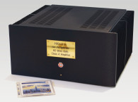
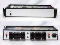
The ax-Amplifier shown in Photo 1 and Photo 2 uses AFEC to achieve ultra-low distortion. Figure 1 shows the block diagram for the project and Figure 2 shows the front end and AFEC amplifier stages. The power amplifier (A1) feedback resistors R38 (Rf), R37 (Rg) in conjunction with the balanced input amplifier, set the overall amplifier gain to 32dB. The junction of these resistors feeds into the low impedance inverting input (A) of the junction of R49 and R50 shown in Figure 2.


With AFEC, a second set of feedback resistors, made up by R4, R11//R8 and R12, tap off the output and are set to the same gain ratio as the main feedback resistor pair. The reference signal for the AFEC amplifier is also the input signal to the power amplifier and is derived from the output of A2, a balanced to single-ended amplifier/buffer. AFEC amplifier A3 compares the reference signal to point (B), extracting from the power amplifier output any residual closed loop distortion as an error voltage at point C. This error voltage is then converted into an error current by R10//R83 (135Ω) and injected into the main CFA low impedance inverting summing node at A along with the primary feedback signal from point D. The AFEC amplifier is compensated with R13 and C4 optimized in LTspice for no overshoot on a square wave input, and checked on the three prototype builds during development.
The error amplifier feedback network is trimmed to match the main feedback gain ratio set by Rf and Rg. If not, the potential worst-case gain mismatch between amplifiers in a stereo set-up with 1% tolerance resistors can approach ~4% or 0.32dB, which some may find unacceptable. The trim is achieved via R4 (1k 25-turn trimmer) giving ±5% adjustment. In volume production, one could specify the AFEC feedback resistors at 0.1% to avoid trimming. Since these are 1206 surface-mount devices (SMDs), the cost impact would be minimal. To prevent extraneous noise pick-up, the AFEC amplifier is physically compact, requiring SMD components, and located well away from high-current signal and power paths.
Unlike feedforward error correction discussed in Reference 1 in which distortion is nulled through cancellation, AFEC distortion reduction is asymptotic and behaves more like conventional feedback. See Reference 2 for further description and Reference 3 for an example of a commercial amplifier utilizing the technique. In this specific implementation, without AFEC, the distortion of the power amplifier at mid-power levels is 25ppm ~ 30ppm, rising to around 50ppm (0.005%) at 70W RMS output into 8Ω, and around 150ppm (0.015%) at 240W RMS into 2Ω. At rated power into 8Ω, AFEC reduces measured distortion by 13 times to 3.5ppm and at >200W output into 2Ω to 12.5ppm. (More information will be available in the Measurement section found in Part 2 of this article.)
The peak current from the AFEC amplifier flowing through R10//R83 is around 4mA at low frequency and about 4.5mA at 20kHz. Without the bandwidth limiting filter on the front end and with an implausibly fast rise/fall time of 1µs at full power, the peak current will approach 12mA and the diamond buffer (DB) will go into Class AB operation during fast signal transitions. However, the bandwidth limiting filter on the amplifier input, and the bandwidth limiting of source material, mean that the input DB always remains in Class A in normal operation. Although the OPA1642 is operating in Class AB mode at these current levels, the distortion is extremely low and at sub 1ppm levels.
An anti-saturation network (D1, D4-D8) connects across R13 and consists of six off BAS21J low capacitance diodes arranged in anti-parallel. Under all normal operating conditions in a CFA power amplifier such as this, the DB and transimpedance stage (TIS) must always remain in Class A. The anti-saturation network limits the AFEC drive current into the inverting summing junction to about 12mA peak or three times the nominal operating current (versus close to 40mA without the clamping circuit) and limits the peak current in R69 and R90 (the DB collector load resistors) to about 6mA (up from about 950µA in the non-clipping state).
The rail sticking associated with hard clipping without the clamping network is about 2.5µs, but with the clamping network it remains ≤1µS at all frequencies. At very high output powers, there is a small 1ppm to 2ppm distortion penalty as a by-product due to the nonlinear capacitance and leakage current of the anti-saturation diodes, but this is a price worth paying for clean clipping. It should be noted that the speaker protection module will quickly disengage the output if the amplifier sustains hard clipping for more than ~2 seconds; clipping in any power amplifier is almost always accompanied by output DC offset.
Front End and AFEC Amplifier Stages
The power amplifier front-end and AFEC amplifier circuit are depicted in Figure 2. The ax-Amplifier accepts a balanced input signal via J3, which is capacitively coupled with C27 and C3 (4.7µF 50V film capacitors) to a conventional balanced to single-ended buffer/amplifier configured around U1/1, half of an OPA1642 dual high-performance Texas Instruments (TI) JFET input op-amp. C5 (270pF COG/NPO) in conjunction with R16 and R17 (1.8k each) sets the input signal -3dB bandwidth to 160kHz.
The common-mode rejection ratio (CMRR) of this simple input stage is 34dB worst case, but if the resistor pairs R18+R19 and R20+R21 are matched to within 0.1%, leaving R16 and R17 as 1% devices, the CMRR improves to 54dB worst case. On my three development builds, the measured CMRR with 1% resistors was 45dB up to 20kHz. The output of the buffer amp is coupled to the input of the power amplifier via R15 (270Ω) and the AFEC amplifier U1/2 through R14 (270Ω) via a 22µF bipolar capacitor, C1. Error correction can be disabled by opening the flash pads U13 and U14 in the practical implementation and these can be used for debugging purposes.
To trim the amplifier output DC offset to 0V, an offset current derived from R5 (25 turn 10k trimmer) and R27 (100k) is injected into the junction of the input DC bias resistor chain comprising R42 (15k) and R30 (270 Ω) while C9 (10µF) provides filtering. Note, the offset bias must be trimmed out before U13 and U14 are flashed closed. The amplifier output offset adjustment range is approximately ±1V. R41 (4.7Ω 1W SMD) isolates the noisy system ground from the front-end signal ground, further improving the amplifier’s already very good noise performance. See Reference 4 on amplifier wiring practices for low noise. Note that once the amplifier offset is trimmed out, the AFEC amplifier will act as a servo and maintain output offsets to very low levels.
The front end of the power amplifier borrows heavily from an earlier CFA design of the author [5]. Q9 and Q10 along with Q5 and Q8 (BC546B and BC556B devices) are configured as a DB. The junction Q9 and Q10 base is the high impedance non-inverting input and the junction of R49 and R50 the low impedance inverting input. The output of the front-end is a complementary current at cascode transistors Q4 (BC546B positive side) and Q7 (BC556B negative side) collector.
The DB input stage operating and output standing current is nominally 950µA and set by 15V Zener diodes D2 and D3 with resistors R46+R40 and R39+ R45, each string totaling 15.15k. R39, R40, R49 and R50 (150Ω) ensure that any Vbe differences between the transistors are swamped by the approximate 145mV stand-off voltages set by the operating currents. Cascode transistors (Q4 and Q7) maintain ~15V across the DB output transistors Q9 and Q10, optimizing thermal balance and DC operating conditions across all four devices.
The discrete front-end bandwidth without input filtering is >40MHz and there is ample opportunity given the extensive use of emitter followers in the DB for oscillator structures to form leading to parasitic high-frequency oscillation. To suppress this, R69 and R70 (1k) are located close to the cascode transistor collectors, while R15 (270Ω) and R31 and R32 (1k) serve as base stoppers. The front-end output current develops 1.75V across load resistors R47 and R48 (1.8k), which provides the DC bias for the TIS stage at DRV TIS+ and DRV TIS-.
The amplifier output voltage (Vfb) is converted to a current by means of Rf, a 1k 5W non-inductive resistor (R38) and injected into the junction of R49, R50, with 33 Ω gain setting resistor Rg (R37) to ground. During normal operation the changes in the DB output current around the nominal 950µA standing current in the closed loop condition are about 80µA pk-pk for low-level sinewave signals and about 450µA pk-pk at full power below clipping. At high frequency, most of this current flows into the compensation network capacitors C22, C23 and C24. Under all normal operating signals, output loads and power, neither half of the DB stage nor the TIS is ever driven into cut-off (i.e., always operates in Class A mode). For further information on DB operation and behavior under transient conditions, see Reference 6.
TIS and Output Stage
Figure 3 shows the TIS (also called the voltage amplifier stage or VAS). The TIS is formed by Q6 (BC556B) operating as a “beta helper” and TIS output transistor Q11 (KSA1381) for positive half signals, while the negative half is taken care of by Q3 (BC546B) and Q12 (KSC3503). R6 and R7 provide emitter degeneration and set the TIS standing current at approximately 12mA. As with the front-end emitter followers, R34 and R35 (1k) suppress possible high-frequency instability. R33 and R51 (1k) emitter resistors are also kept low at 1k for stability reasons [7]. The TIS transistor (Q11 and Q12) collectors are tied together by the output stage bias controller circuit comprising Darlington pair Q1 and Q2 (BC847C SMD devices) and will be discussed in more detail later. Q11 and Q12’s collectors feed the driver transistors Q14 (MJE15032) for the positive side and Q13 (MJE1503) for the negative side.

The output of the driver stage is coupled to four pairs of NJW3281/NJW1302 200W 15A output power transistors (Q15 through Q22) using 4.7Ω 1W base stopper resistors (R53, R55, R58, R59, R65-R68). By utilizing four pairs of devices, thermal stress on the transistors is minimized, and dissipation is better spread across the heatsink. R61-R63, R57, R56, R60, R64 and R54 (0.33Ω 5W) provide emitter degeneration linearizing the output stage. In conventional Class AB and some Class A designs, thermal feedback is used as the primary output stage standing current control mechanism in which the emitter degeneration resistors play an important stabilizing role. In this design, the output stage standing current is directly regulated, improving output stage standing current stability despite the high-power dissipation and thermal cycling. Diodes D6 and D7 provide a current path to the rails should the output devices become reverse biased due to inductive kickback from the speaker load.
Output current overload is detected by sensing the current across a pair of degeneration resistors (R54 and R64) and feeding this to opto-isolator U10 (VO617A-2XO17T) which then drives the Ilim output (U11) via R73 (15k). The peak fault trip current is set at ~26A by means of R71 and R72, so 6.5A peak per output pair.
The amplifier is coupled to the output terminals through L1, a 0.8µH inductor, in parallel with a 2.2Ω damping resistor (R29). This isolates the output from cabling and speaker capacitive loads at high frequency and plays a crucial role in ensuring the ax-Amplifier can drive highly reactive loads (see specifications, Table 1) without stability problems. A Zobel network, comprising R28 (10Ω 5W) and C21 (0.1µF 250V) further ensures that the load reflected to the output devices remains resistive at high frequency, and in combination with the 4.7Ω base-stopper resistors, assures freedom from output stage high frequency instability.

Each PCB module supply rail is decoupled with two off 1000µF 50V capacitors (C17 and C18 for the positive rail and C19 and C20 for the negative rail). These, in conjunction with the 0.1µF SMD ceramic devices (C12 through C16 and C28) keep high-frequency signal currents localized around the output stage.
Bias Controller
The bias controller senses the output standing current across the output stage emitter degeneration resistors with emitter of Q21 the positive tap off point. The nominal bias controller voltage drop from the base of Q2 to the emitter of Q1 is 2Vbe and this cancels the 2Vbe voltage drop across the PNP output stage driver (Q13 MJE15033) and the associated output devices (NJW1302). Thus, the bias controller effectively senses the voltage drop across the output degeneration resistors, and by using an appropriately sized scaling network (R24, R23, R22 and R2), the output stage standing current can be set and controlled. The use of SMD devices for Q1 and Q2 (BC847C), which are in close thermal proximity to the output and driver transistors results in accurate and stable control of the selected standing current as detailed in Table 1.
J5 “Bias” connects to a three-position ON-OFF-ON toggle switch, allowing selection of Class A, Class AB, or Class AAB operation. R2 is used to fine trim the Class A operating current to 550mA per pair. C7 (220µF 6.3V) ensures that at low frequency when the amplifier is driven close to the positive rail, the bias control voltage appearing across Q1 C-E is maintained. Without C7, the bias voltage collapses and low-frequency distortion increases. C2 (220µF 6.3V) decouples the bias controller output and ensures it is not modulated by current changes in the TIS stage, which can lead to increased distortion. Figure 4 shows the measured output stage standing current stability for the completed amplifier from ambient to operating temperature for the three-output stage operating currents.

If the switch attached to J5 “Bias” has either Class A or Class AAB selected, the output stage current will be set accordingly. With Class AB selected (center OFF position), the standing current will not be changed. After the input signal to the amplifier ceases, Q24 will switch off and C29 will discharge through R77 (4.7MΩ) and the amplifier reverts to Class AB after 40 seconds. The bias controller activation time is <2ms for 0 to 10V output transition. R75 and D8 ensure the gate of Q25 cannot exceed 15V, while D9 protects Q24’s base from being driven above the +ve supply rail due to C30 being charged on high output voltage swings. J6 is wired out to a common anode bi-color LED to provide a convenient status indication of the amplifier output stage bias current.
Amplifier Loop Gain and Feedback Characteristics
Figure 5 plots the simulated loop gains for just the power amplifier (teal trace) and for the composite amplifier (red trace) comprising the power and AFEC amplifiers. Below 1kHz, AFEC adds >40dB loop gain, while at 20kHz, it contributes 35dB. Most audio measurement systems have limited bandwidth (usually 48kHz or 96kHz), so accurately measuring the benefit of AFEC at high frequency is problematic since only the low-order harmonics can be included. However, a 19+20kHz IMD test stimulus at high power will reveal high frequency nonlinearity as a 1kHz (and multiples thereof) intermodulation signal. Without AFEC, the ax-Amplifier residual at full power is -95dB down on the stimulus tones, and with AFEC -118dB, a significant 23dB improvement.

Beside the AFEC feedback loop, there are two feedback loops around the power amplifier. The first is the main feedback path via R38 and the second TMC inner compensation feedback loop via C22, C23, C24 and R36. At LF, the compensation feedback path (as opposed to the main feedback path via R38) is from the amplifier output to the input of the TIS via R36 and C22 and C23, with the high reactance of C24 bypassed by R36 (1.8k), thus enclosing the output stage within the loop, and lowering distortion. As frequency increases, the reactance of C24 reduces, approaching the 1.8k of R36 and then at high frequency where its reactance is much lower than 1.8k, transitioning the output stage out of the compensation feedback loop. The amplifier thus reverts to conventional single pole Miller compensation at high frequency with the attendant gain and phase margins required for stability along with dramatically lower distortion.
TMC has the same dual slope characteristic as two pole compensation (TPC) with the loop gain decreasing at 40dB/decade some way beyond the -3dB loop gain cut-off frequency but reverts to 20dB/decade at high frequency before crossing the unity loop gain frequency.
In the non-AFEC system (teal trace), phase margin reduces from 180 degrees at low frequency to ~50 degrees at 20kHz before increasing again, peaking at about 70 degrees before dropping to 63 degrees at the unity loop gain (ULG) crossover frequency at 1.9MHz. With AFEC enabled, phase margin decreases more rapidly as expected, reaching -40 degrees at ~200 kHz before peaking at ~42 degrees at the ULG frequency. Although 42 degrees may seem low, the output coupling inductor ensures that the ax-Amplifier can drive highly capacitive loads without problems. (More information will be available in the Measurements section of Part 2 of this article).
In this design, the 40dB/decade slope occurs from ~20kHz up until ~600kHz, beyond which it reverts to 20dB/decade up to the unity loop gain frequency of 1.5MHz. Unlike TPC, TMC does not display closed-loop high frequency peaking, which in TPC designs may require mitigation [8]. A jumper on the PCB (J4 “COMP”) can be removed to disengage TMC, in which case the amplifier reverts to standard Miller compensation.
Photo 3 shows an inside view of the finished ax-Amplifier with the connectors and one of amplifier channels. The ax-Amplifier will drive any resistive load above 2Ω (lower test limit) in parallel with any capacitance of up to 2.2uF (upper CLoad test limit) with worst-case phase margin of 42 degrees.

Next Month
Part 2 will discuss the power supply, construction for low noise, and measurement results.
Click here to read the second part of this article
Author’s Notes:
Readers wishing to build the ax-Amplifier can purchase the PCBs at www.hifisonix.com.
For US-based builders, the ax-Amplifier housing is available at diyAudio.com and for European builders, directly from Modushop.
References
[1] R. Cordell, “A MOSFET Power Amplifier with Error Correction,” Journal of the Audio Engineering Society, Volume 32, No.1/2, January/February 1984,
cordellaudio.com/papers/MOSFET_Power_Amp.pdf
[2] A Russell, “Augmented Feedback Error Correction (AFEC) for Audio Amplifiers,” 2012 updated 2014, Hifisonix,
https://hifisonix.com/power-amplifiers/error-correction-feedback-system-for-audio-amplifiers
[3] “Product Description - Model 1721, Ovation High Fidelity, www.ovationhifidelity.com/product/model-1721
[4] A. Russell, “How to Wire-up an Audio Power Amplifier,” Hifisonix, July 2015, updated January 2019, https://hifisonix.com/technical/ground-loops
[5] A. Russell, “Hifisonix kx2-Amplifier,” hifisonix, 2021, https://hifisonix.com/projects/kx2-classa-amplifier
[6] A. Russell, “Investigating the Diamond Buffer Input Stage in a Current Feedback Audio Amplifier: Does it Operate in Class A, B or Class AB Mode? Hifisonix, 2017,
https://hifisonix.com/power-amplifiers/current-feedback-amplifier-input-stage
[7] D. Feucht, “Why Circuits Oscillate Spuriously, Part 1 : BJT Circuits,”
audioworkshop.org, https://audioworkshop.org/downloads/AMPLIFIERS_OSCILLATION_BJT_CIRCUITS.pdf (See specifically the section on “Impedance Gyration Viewed from the Emitter”)
[8] B. Cordell, Designing Audio Power Amplifiers, McGraw-Hill, 2011, pp. 177-183
This article was originally published in audioXpress, April 2024