This post as been updated September 22, 2017.

The article revolves around the question whether the term ‘current feedback’ is correctly applied to a ‘CFA opamp’. MK recalls that the term ‘current feedback’ used to denote a feedback configuration where the feedback signal was derived from the output load current. With the advent of the ‘CFA architecture’, however, this term has obtained a different meaning, to indicate not how the output signal sample was obtained, but rather how the output sample is thought to be fed back. This happens often in fast-paced technological fields; but you can’t turn back history so it has to be accepted.
MK explains (correctly) the historical meaning of the term, but then proceeds to argue that this is not correct, based on the definition of current feedback not in the context of a CFA but when viewed from the context of feedback configuration classifications. But as noted, the terms ‘CFA’ and ‘VFA’ in the context of ‘CFA opamps’ have a different, widely understood and accepted meaning and as such are, by definition, correctly applied.
We regret that editing errors have crept into the article. Specifically, eq (1) was printed incorrectly; the original equation was of the correct form Vout = iN * Req//(1/sCeq). Also, fig 2 was inadvertently replaced by a copy of fig 6; the correct fig 2 appears at the corrections link given above. We offer our apologies to author Kiwanuka and our readers alike. A complete correct version of the article is now available here, together with a sample of the exchange between Walt Jung et al and Michael Kiwanuka, posted below. AX
Response from Walt Jung and Sergio Franco to Michael Kiwanuka’s article.
Recently, AudioXpress published an interesting article on the use of feedback amplifiers. The article is Michael Kiwanuka’s “Current Feedback and Voltage Feedback Fallacies” which appeared in June 2017, p32-37. The article purports to clarify certain ‘fallacies’ regarding four basic feedback configurations, using op amps.
The conclusions reached by the article really are most curious. Quoting directly from the final summation: ‘The terms “current feedback amplifier” and “voltage feedback amplifier” as presently used are wholly unfounded. ‘
This is a very odd conclusion, as it flies directly in the face of 3-4 decades of current feedback amplifier (CFA) history! In the attachment cited below, the bibliographic references document this point quite well, and will serve as Useful Background Reading. After careful study, readers should then be able to draw their own conclusions as to whether the feedback system used in conjunction with a given amplifier architecture employs current or voltage. A couple of CFA data sheets will help immeasurably, of course. In fact, this exercise should show just how CFAs operate.
Author MK also is critical of certain book authors on these subjects, namely Professor Sergio Franco and Walt Jung. Accordingly, we have authored a technical rebuttal document, cited below. This document is supported by other signatories, as noted within.
Click to read the Updated technical rebuttal document for the “Current Feedback and Voltage Feedback Fallacies”, Michael Kiwanuka, AudioXpress, June 2017, p32-37. (also available as a downloadable attachment at the end of this article)
Refutation of Jung Et Al.
Michael Kiwanuka
Mr Jung et al, In their rebuttal, Jung et al. state: “So, if you ground the CFA’s noninverting input, break the loop at the CFA’s output, and inject a test signal into the feedback network to see what comes back to the CFA’s inverting input, you see just a current; no voltage is fed back. This is due to the current being injected into a node of zero impedance. In other words, the input buffer keeps the CFA’s inverting input fixed at 0 V, for all current levels. So, you can only refer to this state of affairs as ‘current feedback’ ”.
The above statement is grievously incorrect, for it is an over-simplification that is at the heart of everything that’s wrong with the so-called “current feedback” paradigm. The input impedance at the inverting terminal of the circuit is that of a common-base stage as far as the loop-transmission path is concerned. This will always be a finite input impedance and must never be assumed to be zero, even in theory. Therefore, loop-transmission is essentially the voltage gain of a common-base stage, being mindful of the poor voltage coupling factor between the feedback network and said common base stage as well as the load at the output of the current mirrors.
The forward-path voltage gain of this lamentable circuit is essentially that of a degenerated common-emitter stage, and the egregious error made by Jung et al. is to ignore this very elementary fact and simply assume that the gain in the circuit is due to push-pull current variations in the complementary common-emitter stages merely being passed on to the load at the output of the current mirrors at unity gain.
Additionally, the forward-path of the so-called “current feedback” amplifier takes a voltage as its input and delivers a voltage at its output; therefore, since the feedback network takes the form of a voltage divider draped across the amplifier’s output, the voltage divider must, of necessity, feed a portion of the output voltage back to the inverting input of this circuit, and, alas, allusions to transimpedance gain within the circuit are misconceived. No-one, as far as I am aware, has, for example, ever called the series-shunt voltage feedback pair of figure A1 below (shown without biasing components) a current feedback amplifier, although it operates according to the same principles as the so-called “current feedback” circuit of my article’s figure 1. The series-shunt voltage feedback pair of figure A1 is exhaustively and rigorously analysed by Waterworth [1] in precisely the same way that I analysed the so-called “current feedback” circuit of my article’s figure 1.
Therefore, my equation 2, which Jung et al. denounce, without rigorous justification, as being “based on the wrong premises” and “preposterous”, correctly gives the forward-path gain of that circuit, and it is their equations and those of the authorities they cited that are, in fact, founded on incorrect suppositions and are wholly incorrect. This equation demonstrates that the term “current-feedback” as applied to this hapless topology is a complete misnomer. Indeed, Jung et al. make the cardinal error of assuming the input impedance of the input stage at the inverting terminal of the circuit tends to zero in analysing my equation 2. SPICE in the form of SIMetrix will later be used to dispose of this wholly unjustified over-simplification.
In respect of my equation 2, I, moreover, find it shocking that Walt Jung et al. fail to make the distinction between the forward-path gain and closed loop gain of the so-called “current feedback” topology. The forward-path gain of any amplifier is its gain from input to output with the negative feedback loop opened, but, crucially, with due account being taken of the loading of the disconnected feedback network on the amplifier; the precise method of analysis is eruditely explained by Waterworth [1] and Horrocks [2].
Note carefully that an amplifier’s forward-path gain is not its open-loop gain; this is a very common misconception. Contrary to what is said in Jung’s [3] and Franco’s [4] literature on operational amplifiers, the open-loop gain is, in fact, the gain around the opened feedback loop with the disconnected feedback network in situ; this is also called the return ratio of the amplifier, and, contrary to Hurst [5], it is, in fact, equal in magnitude to the amplifier’s loop gain, although one is the negative of the other. That the open-loop gain of a feedback system and the modulus of its loop gain are one and the same may be confirmed by perusal of any Control Systems textbook.
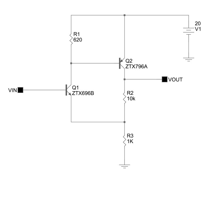
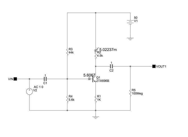
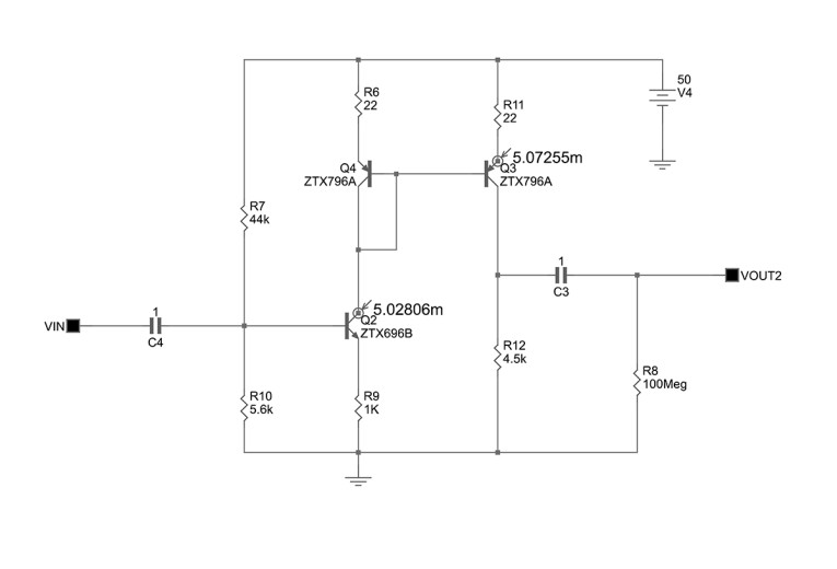
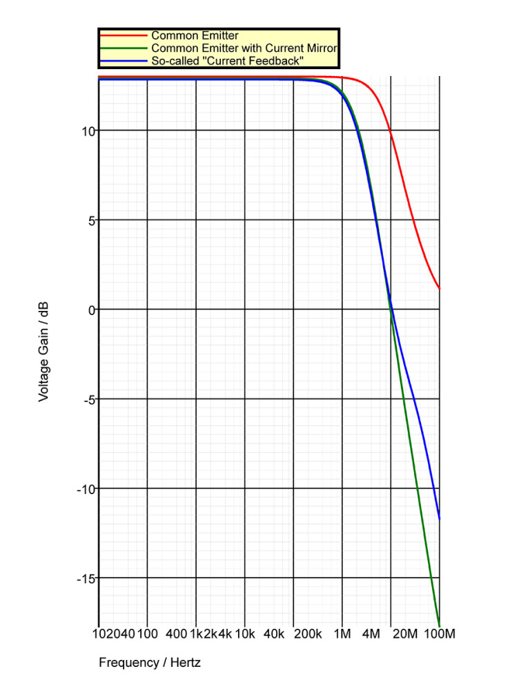
The circuit of figure A2 is a simple degenerated common emitter stage as it appears in SIMetrix; this circuit has an inverting gain of about 13dB. The circuit of figure A3, however, is the same common emitter stage with its output level shifted and inverted again by a current mirror to give the same gain of 13dB using the same load resistor; this demonstrates the elementary notion that, apart from phase inversion, the current mirror merely level shifts the output voltage generated by the voltage gain of the common emitter stage from its collector to the output of the current mirror.
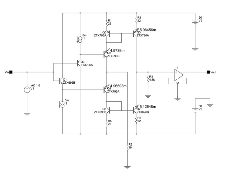
That this is exactly what happens with the so-called “current feedback” amplifier is demonstrated by the circuit of figure A4, which possesses precisely the same emitter degeneration resistor R2 and load resistor R3, at the output of the current mirrors, as the first two common-emitter stages of figure A2 and A3. The circuit of figure A4 is a so-called “current feedback” amplifier, and it gives virtually the same voltage gain of 13dB of the common-emitter circuits figure A2 and A3. This voltage gain is the forward-path gain of the amplifier if it’s assumed that its degeneration resistor R2 is equal to the parallel combination of the series-applied, shunt-derived voltage feedback divider resistors used as the feedback network in my article’s figure 1. This proves that my equation 2 is unambiguously correct, contrary to Jung et al. Note that the frequency response (figure A5) of the circuits of figure A3 and figure A4 are somewhat curtailed compared with that of figure A2; this is due to the pole introduced by the current mirrors.
If series (voltage) applied negative feedback is used, then the voltage applied to both inputs (the base and the emitter of each of the complementary common-emitter transistors of the so-called “current feedback” amplifier of my article’s figure 1) will be of the same polarity, and it is the difference between these two voltages that is amplified by each common emitter stage. Note carefully that although it appears that the input circuit acts as a unity-voltage-gain buffer, driving the potential at the inverting node to that at the non-inverting node, this perspective is incorrect. In fact, with the series (voltage) applied, shunt (voltage) derived feedback network in situ, the voltage at the inverting node follows that at the output of the amplifier, courtesy of the control exercised by the negative feedback.
The negative feedback merely forces the output of the amplifier to deliver whatever current is necessary to the feedback network to drive the inverting input to that potential which, when subtracted from the potential at the non-inverting input, generates that error voltage that is required to drive the amplifier’s forward path to cause it to generate the demanded output voltage. Incidentally, note that the feedback becomes positive if the voltages driving the base and the emitter of each of the complementary common-emitter transistors of the so-called “current feedback” amplifier of figure 1 in my article are of opposite polarity.
The inevitable mismatch in input impedance between the non-inverting input and the inverting input and the resulting difference in the current sourced or sunk by those inputs does not imply that the design of my article’s figure 1 is a current feedback amplifier; on the contrary, as I noted in my article, a current feedback amplifier is identified by the transfer function of its major loop feedback network, and it is one in which the feedback network’s transfer function is a dimensionless ratio of the applied feedback current to the derived feedback current.
As previously established, it is an amplifier’s forward path gain, Av , and not its open loop gain, that is used to determine its closed loop parameters. Thus, to determine the amplifier’s closed loop gain, Acl, the well-known expression is:
Acl=Av/(1+AvB) (1A)
Note that equation 2 in my article, the equation for the forward path gain of the so-called “current feedback” amplifier, was derived on the premise that the amplifier is, in fact, a voltage feedback amplifier, and the fact that my equation 2 correctly gives its forward path gain, as proved above, indicates that the circuit really is a voltage feedback amplifier.
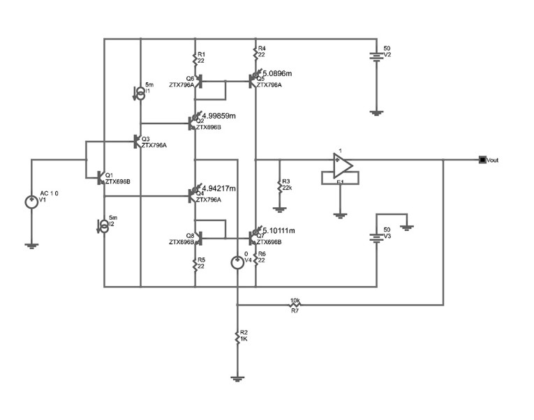
To further demonstrate that the so-called “current feedback” amplifier really is a voltage feedback amplifier because of its series (voltage) applied, shunt (voltage) derived negative feedback network, the DC version (for algebraic brevity) of my equation 2 in my article is substituted into equation 1A above to determine the amplifier’s closed loop gain, Acl. The amplifier used for this purpose is shown as figure A6; as previously established, its forward path DC voltage gain, Av , is simply that of a degenerated common-emitter amplifier, and, with the component designators of figure A6, it is given by:
Av=R3/(R2//R7+re) (2A)
And the feedback fraction, B, is given by
B=(R2/(R2+R7)) (3A)
Where R3=22K
R2=1K
R7=10K
And the intrinsic emitter resistance re=1/gm=1/40Ic=5Ohms, where Ic=5mA is the quiescent collector current of the complementary common-emitter transistors, and gm is their transconductance. Thus, substituting equations 2A and 3A into 1A gives Acl=7.55=17.56dB
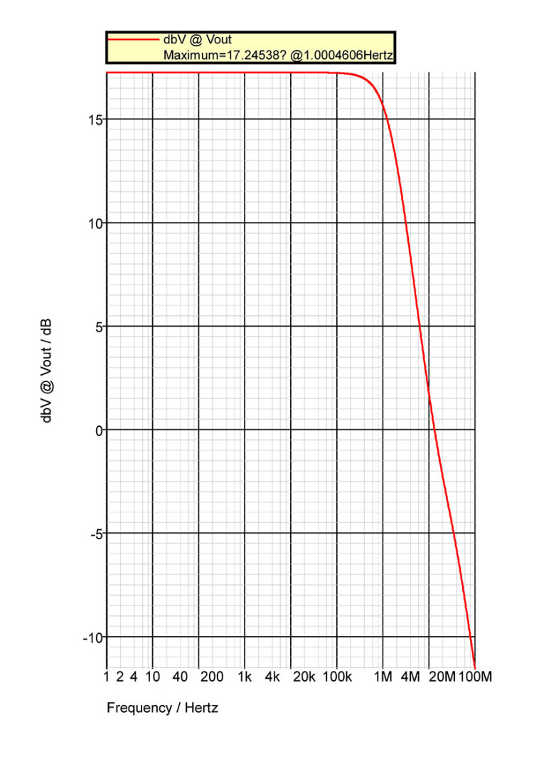
Figure A7 is the small-signal closed loop frequency response of the circuit of figure A6, and it gives the magnitude of the closed loop gain at low frequencies as 17.25dB, which compares favourably with the value of 17.56dB calculated above. Note that the small-signal model used in the calculations above gives results that are accurate to within 10% of those obtained in reality; therefore, the small difference of 0.31dB between the calculated and simulated results is well within the margins of error, and this proves, decisively, once again, that the so-called “current feedback” of figure A6 is, in fact, merely a voltage feedback amplifier. It is also apparent that the voltage feedback amplifier of figure A6, even with the load resistor, R3, removed, is an exceedingly poor design for the following reasons:
- In effect, a single common-emitter stage generates all the forward path gain.
- The loading of the major loop feedback network on the input of the amplifier’s forward path effectively introduces degenerative series (current) derived, series (voltage) applied minor loop negative feedback to the circuit, which reduces its forward path voltage gain.
- Simultaneously, the loading of the inverting input of the amplifier on the major loop feedback network (poor voltage coupling factor) reduces major loop transmission (loop gain).
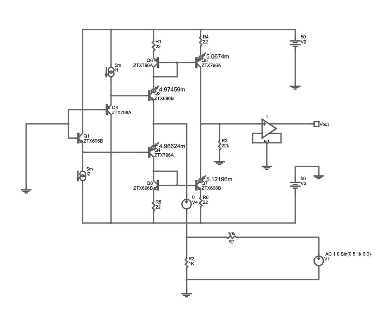
If the non-inverting input is grounded and the feedback disabled by disconnecting the input of the feedback network from the output of the so-called “current feedback” amplifier (fig. A8), then the return ratio of the negative feedback loop may be established by connecting an independent voltage source to the input of the feedback network.
It is suggested by Jung et al. that this demonstrates that the circuit really is a “current feedback” amplifier because the input circuit of the amplifier acts as a unity-voltage-gain buffer between the grounded non-inverting input and the inverting input, driving the inverting input to zero volts. This, however, is misleading because it is strictly only true in the absence of applied signal to the inverting input; moreover, there is no negative feedback to control the potential at the inverting input: the feedback loop, as previously indicated, is disconnected at the output of the amplifier. Therefore, it is wrong of Jung et al. to suggest that this implies that the circuit is a “current feedback” amplifier.
With the non-inverting input grounded, the complementary common-emitter transistors at the input of the circuit are now complementary common-base stages, and the disconnected feedback network constitutes a simple voltage divider across the inverting input (fig. A8). The fact that the lion’s share of the current in the divider goes into the inverting input is simply attributable to the very poor voltage coupling factor (much less than the ideal of unity) between the voltage divider and the much smaller input impedance of the inverting input.
Therefore, the loop transmission of the so-called “current feedback” amplifier, with the non-inverting input grounded, is essentially the voltage gain of a common-base stage, with due account being taken of the load at the output of the current mirrors and the very poor voltage coupling factor between the feedback network and inverting input. That this is, in fact, true, shall now be demonstrated from first principles.
The grounded independent voltage source, V1, in figure A8 generates a 5V(Peak) sine wave at 1KHz. Now, the magnitude of the output voltage of the common-base configuration is given by gm.Vinv.R3, where each transistor’s transconductance gm is approximately equal to forty times the quiescent collector current, which is 5mA in this case. The small-signal change in the base-emitter voltage of each transistor is essentially the voltage Vinv at the inverting input, which is obtained by multiplying the voltage generated by V1 by the voltage coupling factor at the inverting input. The voltage coupling factor is (re//R2)/((re//R2)+R7), where re=1/gm=1/(40*5mA)=5Ohms.
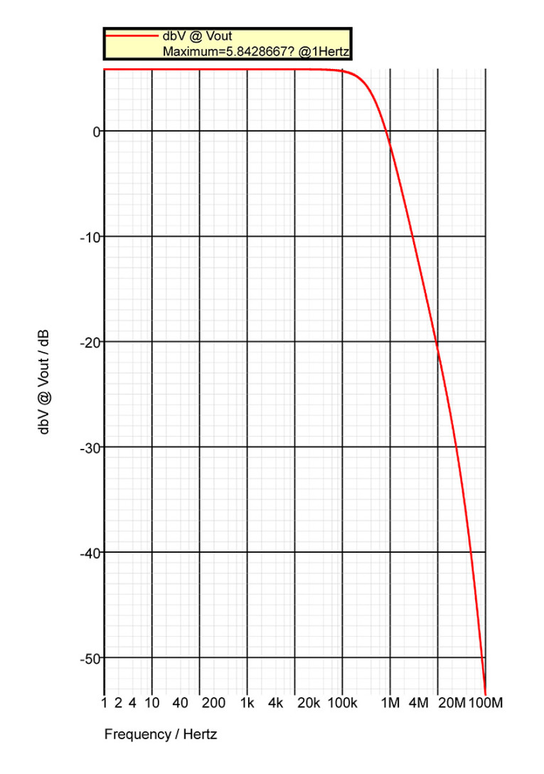
Thus, the voltage, Vinv, at the inverting input calculates as 2.49mV(peak), and this gives the output voltage dropped across R3 as roughly 10.94V(peak). This gives a gain of 6.8dB, and this compares favourably with the gain of 5.8dB given by SIMetrix (fig. A9). Note, once more, that the small-signal T-model used in the calculations above gives results that are accurate to within 10% of those obtained in reality; therefore, the small difference between the calculated and simulated results is well within the margins of error, and proves, decisively, once again, that the so-called “current feedback” of figure A6 is, in fact, merely a voltage feedback amplifier.
Alternatively, it may be assumed that the current sourced and sunk by R2 is negligible, and that, therefore, the feedback resistor, R7, supplies all the current sourced and sunk by the inverting input, and this is simply 5V/10KOhms=500uA. This current drops 11V(peak) across the 22K load resistor, R3, giving a gain of 6.85dB, and it is apparent that this result is virtually identical to that calculated in the preceding paragraph. This simple contrivance has misled many into thinking it justifies referring to the circuit of figure A6 as a “current feedback” amplifier. This is not true, not least because a current feedback amplifier is one in which the negative feedback controls the current in, and not the voltage across, the load connected to the output of the amplifier.
Note, further, that in my article I did not dispute the fact that the so-called “current feedback” topology has certain characteristics that distinguish it from what are erroneously called voltage feedback amplifiers. Indeed, I pointed out that the push-pull class-B operation of the complementary common-emitter input stage of the so-called “current-feedback” circuit makes very high slew rates possible by supplying a relatively large amount of current to charge and discharge the capacitance at the output of the current mirrors; this eliminates the first-order restriction on slewing that is characteristic of the classical “voltage feedback” topology.
However, it was and is my contention that this and other idiosyncrasies attributable to the so-called “current feedback” circuit do not justify referring to that circuit as a current feedback amplifier. Whether a circuit is a current feedback amplifier is and was traditionally established by identifying its negative feedback connections. The so-called “current feedback” topology almost invariably utilizes series-applied, shunt-derived negative feedback, which makes it a voltage feedback amplifier. It is to be regretted and roundly deprecated that so many intelligent people wasted so many decades deluding themselves over this rather pointless topology.
References
1. Waterworth, G., “Electronics” (McMillan College Work Out Series), pg. 111-112, ISBN 0-333-45871-0.
2. Horrocks, D. H., “Feedback Circuits and Op. Amps”, 2nd Edition, pg. 69-82, ISBN 0-412-34270-7.
3. Jung, W., “Op. Amp. Applications Handbook”, pg. 6, ISBN 0-7506-7844-5.
4. Franco, S., “Design with Operational Amplifiers and Analog Integrated Circuits”, 4th edition, pg. 24, ISBN 978-1-259-25313-3.
5. Hurst, P. J., “A Comparison of Two Approaches to Feedback Circuit Analysis”, IEEE Transactions on Education, Volume 35, Number 3, August 1992.


