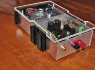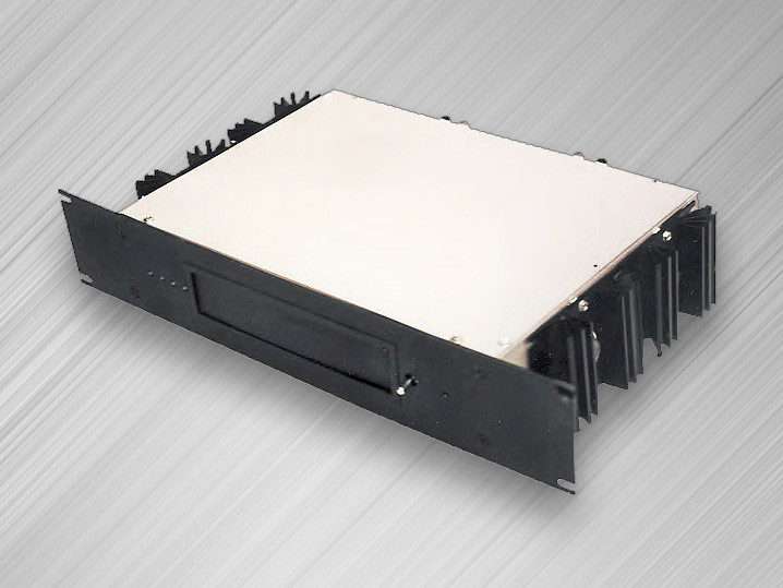
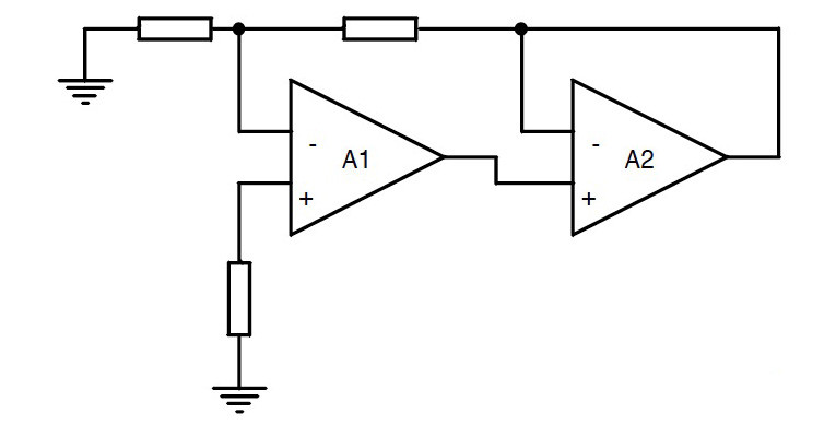
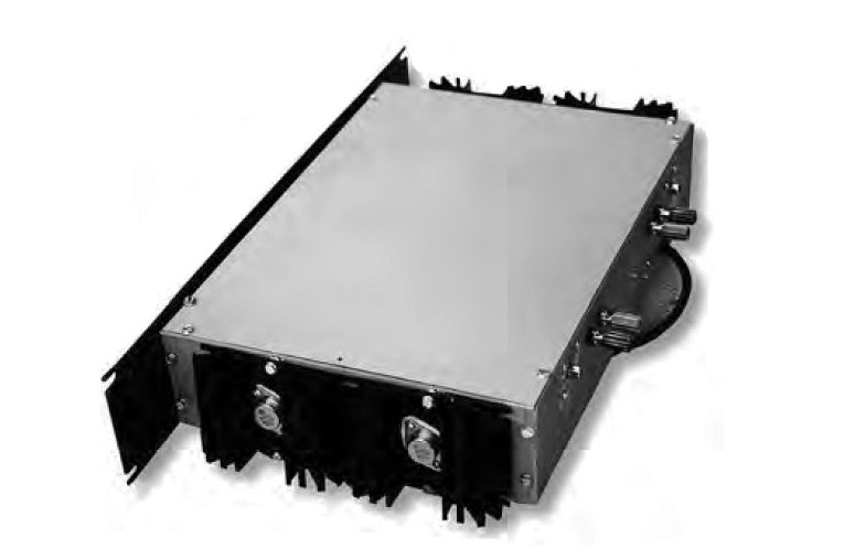
Figure 3 shows the block diagram of the circuitry I used in this project. I relied heavily on information in the 1994 Burr-Brown Applications Handbook (1) to design my amplifier, and the circuit of Fig. 3 is thoroughly discussed in bulletin AB-028, which is the main reason I chose it over the other two. In addition, it seems to offer higher loop gain, a desirable feature here, since my goal is ultra-low distortion. (Photo 1 shows the completed amp.)
Other Features
The composite offers other advantages. For example, you can combine the best qualities of both amps used in the compound, and DC performance of the composite is excellent. Since A2 is in the feedback of A1, the composite retains the DC characteristics of that amp. In fact, because A1 does not drive the load directly, its DC accuracy is better than that of A1 alone. This is an especially welcome feature in a power amplifier.
Thermal feedback in a power amplifier driving heavy loads can cause errors due to self heating, but the composite eliminates this problem. This is not just theory. My composite amplifier has a DC output-offset voltage of ±1mV, stays there regardless of the load placed on the output transistors, and uses no “zero adjustment” pot. Another advantage in my amp is the slew-rate boost: in the composite, the slew rate of A1 is multiplied by the gain of A2.
Obviously, the composite must be stable for you to benefit from its use. With composites, you should include the rolloff characteristics of both A1 and A2 in the AC analysis, and also have some means of providing phase compensation for the loop. Two amplifiers in a loop virtually guarantees oscillation, since the individual poles combine to produce a two-pole rolloff. Fortunately, there is a way to stabilize this composite.
Stability
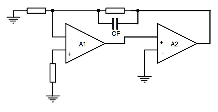
In Fig. 3, A1 and A2 are identical, compensated op-amps, which makes it easy to predict the composite rolloff needed for AC analysis. I have learned from building this amp that the open-loop gains of A1 and A2 need not be the same. However, in this type of composite, it is essential that A1 and A2 have the same unity-gain frequency, FT. At FT, each must have a phase margin of 90°. These requirements are easy to meet if you use a dual, compensated IC op-amp.
Remember, though, that this is to be a 50W power amp, so A2 in this project is a discrete unit to handle the power. Making the discrete amp unity-gain stable at some specific frequency with the required phase margin of 90° turned out to be a tough job. Indeed, most of the design effort in this project was directed toward meeting that requirement.
As things worked out, 2MHz was the highest unity-gain frequency I could achieve in A2 while still meeting the phase-margin requirements. All that’s needed now to complete the composite is a compensated IC op-amp having an FT of 2MHz. For this, I selected the OPA-121. Since this project is a power amp, you must also consider slew-rate needs.
The intended output power is 50W into 8Ω up to 20kHz, which requires a minimum slew rate of 3.55V/μs (2). The OPA-121 has a slew rate of 2V/μs. The composite solves the apparent slew rate shortage of this op-amp because it is multiplied by the gain of A2, as mentioned previously. The voltage gain of A2 at 20kHz is about 130, so the effective slew rate of A1 is 260V/μs.
Unfortunately, I was not able to utilize all that speed because the slew rate of A2 itself is about 12V/μs, and this slew rate sets the power bandwidth of the amp. Referring again to Fig. 3, capacitor Cf stabilizes the composite, but for the stabilization method to work, the closed voltage loop gain of the composite must be ten or greater. I use a voltage gain of 30 in this amp. (Both the mechanism of stabilization, as well as the reason for the minimum gain, require an explanation that is well beyond the scope of this article. I refer you to the previously mentioned application bulletin for more details.)
The size of Cf is found using the following equation:
Cf = √10 Acl/2πR2 FT
where
Acl = 31, R2 = 8200, and FT = 2MHz.
Solving the equation, Cf = 170pF. I used 180pF. You can determine the amp’s bandwidth by using the value of Cf and R2 in the equation, Fbw = 1/2πCf R2 = 107kHz. You now have almost enough information to make a Bode-plot of the composite amplifier. All that’s missing is the open-loop gain (Aol) specs for A1 and A2. Aol for the OPA-121 is typically 120dB, and for A2, it’s 78dB. The Bode plot of the amplifier is shown in Fig. 4.
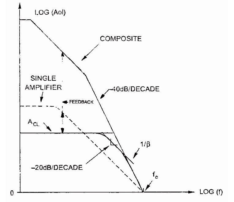
Bode Plot
In Fig. 4, the heavy, solid lines are for the composite amplifier. For comparison, the dotted lines show the AC characteristics of a typical conventional power amp operating with the same closed-loop voltage gain. At any given frequency, the difference between Aol and Acl is the amount of global feedback. The more feedback, the less distortion.
This Bode plot provides a visual display of the superior distortion-suppressing capabilities of the composite arrangement. The Acl of the composite is down 3dB at about 105kHz, which is the effect of the stability capacitor, Cf, which rolls off the response of the composite so that it eventually intersects the Aol curve at a rate of 6dB/octave, ensuring stability.
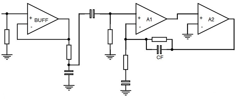
The 105kHz bandwidth is too wide for the best low-noise performance (3). I would prefer it to be about an octave lower. Normally, it is possible to restrict bandwidth by using a small capacitor across the feedback resistor, but in this composite that space is already occupied by Cf. So I added a unity-gain, low-pass, active filter ahead of the composite.
The active device also serves as a buffer. The preamp used with this power amp is an unknown factor, and its source resistance could interfere with the filter were this buffer not included. In addition, the 10kΩ input resistance may be too low for some preamps, and the buffer permits you to substitute a more suitable load.
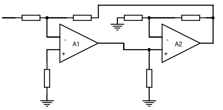
The active device here is the 5534 opamp, a very quiet unit that also sets the noise figure for the amp. Figure 5 shows the full block diagram of this amp with the buffer/active filter included.
Amp Circuit
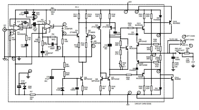
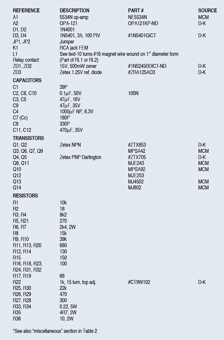
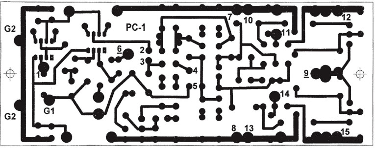
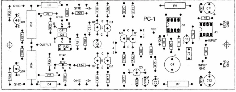
Figure 6 is the amplifier’s detailed schematic. Table 1 shows the parts list. Figure 7 is the circuit layout, and Fig. 8 is the amp stuffing guide. Most of the circuitry is conventional and requires no explanation, but there are a couple of exceptions. Transistor Q8 provides temperature compensation for the output-stage bias current. It is physically connected to the case of Q11 with a short 4-40 machine screw and hex nut.
Bias current should be adjusted for optimum class-B operation at 11.5mA using R22. Single-slope volt-amp limiting is provided by Q9, Q10 with associated circuitry of D1, D2 and resistors R25–30. The amplifier output is routed to the speaker jack through normally open relay contact, “R,” shown here as a SPST switch.
Power Supply
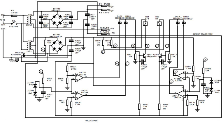
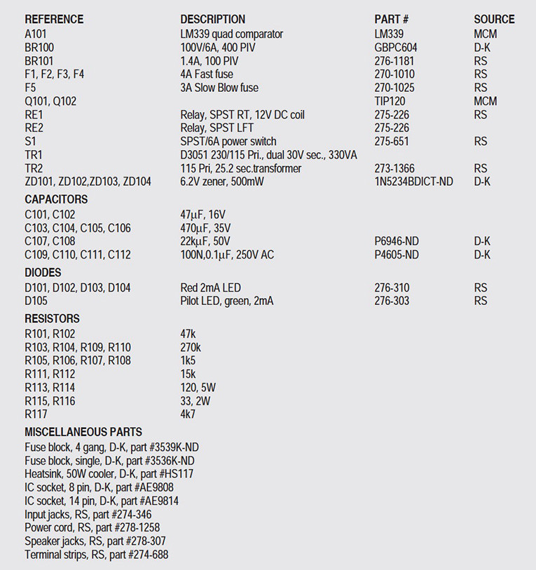
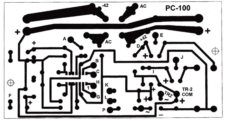
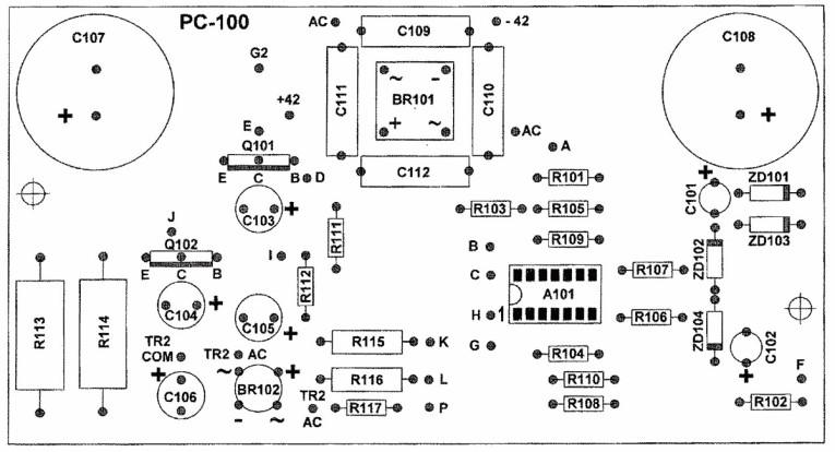
Figure 9 is the schematic of the power supply and relay pull-in circuits. Table 2 shows the parts list, Fig. 10 is the PCB layout, and Fig. 11 is the stuffing guide. A101 is a quad comparator with two comparators per channel used to sense the DC-output offset condition of the main amplifier. One comparator is biased from the positive power supply to +80mV, while the other one associated with that channel is biased from the negative power supply to −80mV.
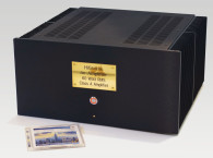
Each of the two comparators shares a common input from the amplifier output via resistor R101 from the left channel, R102 from the right. Capacitor C101 along with R101 and C102 with R102 form low-pass filters to keep the AC portion of the output signal from activating the comparators. As long as the power amplifier output remains within 80mV of ground potential, there is no output from the comparators, and the power transistor associated with that channel (Q101 or Q102) will conduct and pull in the relay for that channel. The outputs of each pair of comparators are wired OR via LED 1 and 2, or LED 3 and 4. I mounted these LEDs on the front panel for visual indication (Photo 2).
The main amplifier circuitry is completely DC coupled, and in the event of a failure the output could settle at a DC output high enough to damage the loudspeaker. The comparator/relay circuit prevents this. I had hoped that this same circuit would also remove all turn-on noise at the instant of power application. Unfortunately, it is not 100% effective for that purpose. Although there is no “thump” when you first apply the power, occasionally there is a soft “tick” or “swish.” There is never any noise when you turn off the power.
As I already mentioned, ultra-low distortion is the goal of this amplifier. As always, it is best to make the amplifier as linear as possible before applying global feedback. British engineer Douglas Self in his excellent book, The Audio Power
Amplifier Design Handbook (4), has identified eight distortion mechanisms in power amplifiers and ways to minimize them. I have taken great care to follow his advice in the design of this amplifier.
Distortion measurements are a problem for me with this amp. For one thing, my own analyzer test set has a residual distortion of about .01%, which is quite inadequate for measuring this amp. On the other hand, better test equipment does not appear to be an answer, either. The huge levels of global feedback used in this amp put the distortion products well into the noise floor, where even the best equipment can’t retrieve them.
Now, how does the amp sound? In a word, invisible. It interfaces so seamlessly between preamp and loudspeaker that it just slowly fades away behind the sound stage, leaving only the music to catch your attention—music that is a step closer to the original.
In the absence of a signal, the amplifier is dead quiet with no audible hum or hiss. With 50Ω source resistance, A-weighted noise is more than 100dB below full-rated output. Maximum power output, one channel driven, 1kHz, 8Ω load, is 75W; and 90W with a 4Ω load under the same conditions. Frequency response at 1W output using the suggested low-pass filter is ±0.5dB, 20Hz–20kHz. Half-power (−3dB) frequencies are 2Hz and 58kHz. Sensitivity is about 650mV for 50W output.
Construction
For a nominal fee the local heating and air-conditioning shop made my chassis. Material is galvanized sheet metal, which is quite ugly, so I primed it with zinc chromate and painted it light gray. Box size is 14″ × 10″ × 3″ with a ³⁄₈″ lip all around the perimeter for attaching the top with hex-head sheet-metal screws. This lip is also provided at the front and back corners of the main chassis.
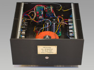
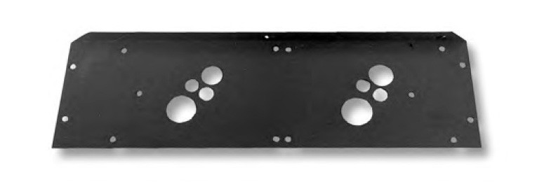
The front, bottom, and back are of one piece of sheet metal, bent in a U shape (Photo 3). Both sides, as well as the top, are separate pieces, attached to the main chassis with ³⁄₈″ × 6 hex-head sheet-metal screws. I rack-mount equipment, so I attached a 3½″ × 19″ faceplate to the main chassis with #10 sheet-metal screws, and reinforced the front corners of the chassis with a 3″ length of 1″-square extruded aluminum tubing. Angle aluminum or iron would do just as well.
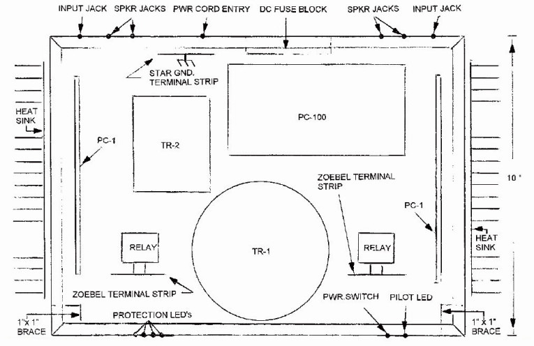
Figure 12 shows where I mounted the major components inside the chassis. Exact spacing between components is not critical and is therefore not included. Moreover, you may prefer to use exotic input/output jacks, which usually take up more space than the ordinary kind. The chassis specified should be large enough to handle custom hardware as well as accommodate any necessary relocation of parts.
Grounding And Wiring
Although minimal distortion is the goal of this project, the highest priority is safety, and for that reason you should use a three-conductor power cord. It is not necessary to sacrifice safety to achieve a system free of ground loops and annoying hum. To do so, I used Radio Shack #274-688 for the star-point ground. This is a terminal with five eyelets, with the middle one having a bracket for attachment to the chassis. I located this terminal close to where the power cord enters the chassis and bolted it to the bottom using #6 machine screws and serrated edge lock washers, scraping the paint off the chassis at this point to get a good electrical connection.
I soldered a short piece of bare wire across the bottom of the terminal strip to tie all eyelets to chassis ground. I crimped and then soldered a ring-type “solderless” connector to the green lead of the power cord and fastened it to the terminal-strip mounting screw with another lock washer and a 6-32 hex nut. It is important that the “cold” or common side of the input phono jack not contact the chassis. The same holds true for the common terminal-output speaker jack.
When you fasten these parts to the chassis, use an ohmmeter to check that they are insulated from it. If you wait until the ground wires are attached to make this measurement, it is not possible to verify this condition. With one exception, all grounding was done with green, insulated, #18 gauge, stranded wire. The center tap of the secondary of the toroidal power transformer is connected directly to an eyelet on the starpoint ground strip.
If you orient parts as shown in Fig. 12, you will need to splice a few additional inches of wire so this lead reaches the intended point. Solder the center-tap lead of transformer TR2 to the “GND” trace on PC 100, which is near the smaller of the two bridge rectifiers on this board. Also on PC 100 is another trace marked “GND” that you must wire to the star point. Because of the width of this trace, it may be necessary to use a soldering gun to avoid a cold solder connection here.
The common side of each phono jack is wired to the star point, as is the common terminal speaker jack. On each amplifier board, PC 1, there are two ground connections, G1 and G2. Wire G1 to the common side of the input phono jack, and G2 to the star point. There are two eyelets on this board marked G2, but only one of them should be used. Use whichever one requires the shorter length of wire to the star point. This will depend on whether you are wiring the left or the right channel, and will become obvious when you do it. These ground leads carry very little current, so I used #24 gauge wire for them.
Capacitor C10 and resistor R35 form a zobel network at the output of the power amplifier. These parts are not on the printed circuit board. I mounted them on another Radio Shack five-eyelet terminal strip. I used one 6-32 machine screw to fasten both this terminal strip and the protection relay to the chassis.
You can solder the zobel network to any of the four ungrounded eyelets. One end of resistor R35 needs grounding, but do not use the terminal strip mounting bracket for that purpose. Ground the zobel network with a wire to the star point. There are more leads back to the star than there are points. Double up wires to the eyelets where you can. If you run out of room, solder to the jumper wire connecting the eyelets together.
This RC zobel network plays an important part in the stability of the amplifier and is needed for that function whenever the amplifier is energized. You must wire it so it is directly attached to the amplifier output at all times, which means it needs to be wired “upstream” of the normally open relay contact. If by mistake you wire it “downstream” of the relay contact, the power amplifier may be unstable for the five or six seconds it normally takes for the relay to close.
Parts Placement
Fasten PC 100 to the chassis bottom using two threaded standoffs. The four unit fuse block for the dual-polarity power supply is fastened to the back plate of the chassis approximately centered behind PC 100. I left enough space between the fuse block and the circuit board to permit easy fuse replacement.
Glue the fuseholder for the 120V AC main power to the top of transformer TR2 with silicone RTV adhesive. The secondary leads of the toroid transformer are long enough to reach their destination on PC 100, but too short to allow easy removal of the board for visual inspection or troubleshooting, so I lengthened these leads by about 4″.
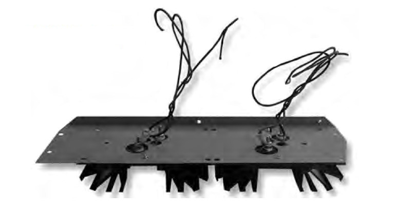
The heatsinks specified are factory drilled for the TO-3 output transistors. Before installing these transistors, place the heatsinks on the 3″ × 10″ end panel (removable in mine) at the desired location and, using a sharp pencil, trace the hole locations of the base, emitter, and collector (case). Use the eyeball method to find and then center punch these holes. Drill them using a ⁵⁄₃₂″ drill bit, and then de-burr. Find the four smallest rubber grommets in the Radio Shack assortment and try one of these in the holes just drilled. If the hole needs to be enlarged, use a test hole in a piece of scrap sheet metal or thin plastic.
Once you find the proper size drill bit, enlarge only the holes for the base and emitter leads. De-burr the enlarged holes and install the four grommets. If they fit too loosely, fix this with silicone rubber glue. Next, enlarge the collector/case holes to 1/4”, then use a universal step bit to enlarge the top hole to 7/16” and the bottom to 3/8” (Photos 4 and 5).
I used mica insulators and silicon heatsink compound between the transistor case and heatsink. Fasten the power transistors to the heatsink using 1″ 6-32 machine screws, nylon bushing, #6 washer, lock washer, and hex nut. I soldered a 12″ length of #24 wire to the base pin, and a 12″ length of #18 wire to the emitter pin. I crimped and then soldered a ring-type “solderless” connector to one end of another 12″ length of #18 wire and fastened it to the upper 6-32 screw with another lock washer and hex nut.
Then thread the base and emitter leads through the grommets and the collector/case lead through the upper, larger hole. Fasten the heatsink to the sheet metal. I found the factory-made flanges on the heatsink inconvenient to use, so instead, I drilled holes at top center and bottom center of the heatsink and used 3/8” × 6 sheet-metal screws to hold them to the sheet metal. The heads of the machine screws holding the threaded standoffs in place prevent the heatsink from pulling up flush against the sheet metal. To overcome this, I used a pair of flat washers as spacers between the heatsink and the sheet metal.
Once this mechanical assembly of the output transistors is complete, you can trim the leads to the appropriate length and then solder them to the correct points on PC 1. The leads from the power transistors should be inserted into PC 1 from the foil side of the board, and then soldered. All other wires to this board should be inserted from the component side.
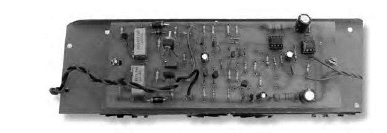
You should orient PC 1 with the input stage near the back or rear of the chassis as close to the input phono jack as possible. Check that this condition exists before completing the wiring for this circuit board. Wiring should be as short and direct as possible and yet long enough to allow easy removal of the board and heatsinks for visual inspection and/or troubleshooting (Photo 6).
Circuit Boards
You should have good soldering skills, be able to read schematic diagrams, and own and know how to use a VOM, signal generator, and oscilloscope if you are interested in building this amp. I’d like to mention a better way to stuff the boards than the method used by most project builders. I divide the circuitry of the amplifier into sub-circuits, or sub-assemblies, according to the function performed. (A typical sub-circuit contains at least two, but rarely more than four, components.) Then I stuff and solder in place the parts of the designated subcircuit, power up the board, and take DC voltage measurements to verify that it is working properly.
I repeat this procedure with the next sub-assembly, and so on, until the board is completely stuffed. A mistake produces a voltage reading significantly different from the one shown for that step, and you can quickly find it since it must lie somewhere in the last two, three, or four components stuffed.
During the stuffing process, the main amplifier board is powered from a dual-polarity, 18V source using the small Radio Shack transformer. The use of a much lower-than-normal supply voltage usually prevents damage to components if you make a mistake. I even use this low voltage supply to initially test the completed amplifier.
Once you know the amp is working properly, replace the board supply with the normal high voltage source. My stuffing procedure is very detailed. It is also lengthy, and so I do not include it in this article.
The finished project takes up a minimum of space. Despite the compact size, the interior is roomy enough to allow easy access to all parts. Moreover, the board layouts are spacious and use no surface-mount parts. Best of all, this amp offers a level of performance one step closer to that elusive goal, a straight wire with gain. Finally, many thanks to Rod Cavin, who supplied all the PC board artwork for this project.
Note:
Most of the parts listed in the parts lists are readily available from any supplier. However, some parts are available from specific suppliers; D-K = Digi-Key, MCM = MCM Electronics, and RS = Radio Shack. All resistors are carbon composition, 1/4W, 5% tolerance, except as noted. All capacitors are radial lead. Main transformer is available from Avel Transformers.
References
1. 1994 Burr-Brown Applications Handbook. (Available from Digi-Key Electronics.) See Fig. 9, p. 202. Burr Brown Application Notes, AB028. (Now available on TI’ website)
2. Jung, Walter, Audio IC Op-Amp Applications, Howard W. Sams, p. 44.
3. Motchenbacher & Fitchen, Low Noise Electronic Design, John Wiley & Sons, Chapter 7.
4. Self, Douglas. also audioXpress, “Distortion in Audio Power Amps, Parts 1-3,” AE 2/99, 3/99, 4/99.
This article was originally published in audioXpress, April 2001.