Introduction
Stuart Yaniger wrote a great article for audioXpress in February 2009, “The ImPasse Preamplifier,” describing a tube preamp to drive a pair of Nelson Pass’ First Watt F4’s (or other low-to-unity-gain power amplifiers) in balanced mono. The F4 is a unity gain amplifier requiring a preamplifier capable of driving the full-expected output swing. As two channels of the F4 should be able to swing 40 V in Class-A, for 100 W of output power, the preamp must be capable of delivering 28.3 VRMS. Yaniger’s preamp is truly an elegant design with very, very low distortion, using a 6SN7 to drive a 6922 in balanced mode. There are LEDs, NE2H neon lamps, and depletion MOSFETs in the design. Enjoy the project! - J. Martins
It all started with the Burning Amp Festival (BAF) ’07 in San Francisco. My friend was building a balanced version of Nelson Pass’s First Watt F4 and asked for a recommendation on how to drive it. The Pass F4 is a unity gain power buffer, meant to take a high-level output from a preamp and drive speakers with it — an interesting concept.
the full expected output swing.
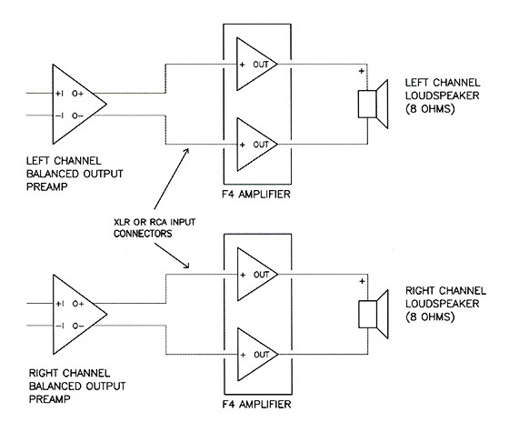
The schematic suggests that the F4 can swing about 20V peak into an 8Ω load single-ended, but 40V peak in balanced mono. A diagram of the balanced mono connection for the F4 is shown in Fig. 1. A preamp with balanced outputs is used for all of the voltage gain and to drive the cables to the power amps, along with the power amp input impedance.
The F4s buffer the balanced preamp outputs and provide a balanced signal to the speakers. Because a unity gain power stage can be designed to run open loop with quite low distortion, the performance of the electronic path rests almost entirely on the balanced-output preamp, which ought to be low distortion and low source impedance to reduce the criticality of interconnects.
So rather than recommend a preamp for the task, I took the totally impractical step (I don’t own an F4!) of designing and building one for his demonstration at BAF ’07. And, of course, it needed to be called The ImPasse.
The Road Not Taken
I will first examine the design requirements. In the balanced mono arrangement, your preamp must be able to swing 20V peak on each of its output polarities, and do that driven from a typical line-level source (2V RMS or 2.8V peak). To accommodate CDs and records that are cut at a lower than normal level, you should build in some extra gain, arbitrarily and conveniently arriving at a target gain of 26dB (A = 20). In the balanced mono connection, the power amplifier input impedances are identical and symmetrical. Thanks to the FET input, their values are also somewhat arbitrary — the intrinsically low gate current of a FET means that voltage offsets due to gate current can be very low even with relatively large gate resistors. This relieves the preamp from the need to deliver much signal current; it just needs to swing many volts very cleanly.
For me at least, the requirement to swing a lot of volts at low current with a simple circuit suggests… tubes. And what’s even more compelling is that tube stages that give balanced outputs at high voltage levels are already well-known and characterized—the input and driver stages of a push-pull power amplifier fit the ticket perfectly (I’ll return to this point at the end).
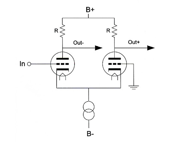
Given the symmetrical loads and the requirements for balance, you have several options. The first that comes to mind is the classic differential amp (Fig. 2). With a constant-current sink in the tail and load that is equal on both polarities, the balance is excellent. Likewise, the output impedance, Zout, can be made relatively low; with symmetrical loads, it is roughly equal to the plate resistance in parallel with the load resistance. Power supply rejection is excellent.
To get to the target gain of 20, you need a tube with a gain somewhat larger than 40; from a single-ended source, gain to each plate of a differential amplifier is half the gain that the same circuit would have in common cathode. Restricting yourself to easily available tubes, you could look at 12AT7/ECC81, 6SL7,
or 12AX7/ECC83. Being more exotic, you could check some of the high gm European pentodes, triode connected, in order to achieve the requisite gain with a low plate resistance.
Consider the common tubes. Of the three candidates, the 12AT7/ECC81 has the lowest plate resistance; at 10-15k for normal operating currents, the preamp’s output impedance will be 20-30k, which is somewhat higher than is comfortable. Any cable capacitance will be liable to cause HF losses. The other tubes produce a much worse problem. It seems that you’ll need to follow the differential amplifiers with a pair of buffers, probably cathode followers, so a well designed preamp based on that topology will have four tubes at a minimum.
You can do somewhat better with the exotics. A D3a, triode connected, will have a plate resistance of slightly greater than 2k at 20mA operating current. This will result in an output impedance of about 4k5, considerably better but still quite high. But with care and attention paid to the cables and amplifier load, this could be a viable option, albeit at some expense — D3a is not cheap, and the current to run two channels of preamp will be 80mA or more.
‘Tis A Gift To Be Simple
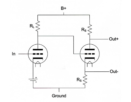
Turning to a different topological option well-trod by power amplifier designers, consider a simple common-cathode voltage amplifier feeding a split-load inverter (Fig. 3). You can couple the two stages in various ways: direct coupling, RC coupling, or a combination of the two are all simple and effective.
Contrary to myth, the split-load inverter has symmetrical source impedance from both the plate and cathode sides as long as the load is also symmetrical. That source impedance is lower than that of a comparable diff amp, being approximately 1/gm (similar to a simple cathode follower). For a common tube such as ECC88, for example, Zout will be approximately 100-200Ω, a much more attractive figure than even the exotic differential amplifier.
Better yet, the overall gain of the combination of grounded cathode voltage amplifier and split-load inverter will have double the gain of the same voltage amplifier tube in differential mode. This extends the range of tubes that you can use for the first (voltage amplifier) stage to include medium-mu triodes such as 6SN7.
Medium-mu triodes also have the advantage of potentially lower input capacitance due to reduced Miller effect. If you use a high mu triode such as a D3a as an input tube, the input capacitance for a single-ended source will be nearly 300pF. This might upset some driving sources, but these days that would be a minority. Still, it is something to consider, especially when choosing the value of the volume control—assuming a low source impedance driving the volume control, the worst-case source impedance is at the halfway (-6dB) setting and is about half the volume control total resistance.
This impedance, combined with the tube’s input capacitance, forms a pole, which will often impinge on the audio band. A 10k potentiometer combined with a D3a input will give a -3dB point of about 100k, which is a satisfactory bandwidth, but higher values could begin to be problematic. Gain is also significantly higher than target, so some careful reduction measures would need to be designed in.
Fortunately, a very common medium-mu triode, the 6SN7, has demonstrably excellent linearity at these voltage swings — the requisite gain, sufficiently low input capacitance (80pF)—and is widely and easily available in an impressive variety of flavors.
Distortion performance is comparable to the exotics, and input capacitance is significantly lower. Among common medium-mu tubes, it is the most linear in voltage amplifier service, and the mu of 20 is spot-on for this application.
Final Answer
So, given the design choices here, I’ve gone conventional and will use a 6SN7 as a single-ended common-cathode voltage amplifier, and an ECC88 as a split-load phase splitter/buffer. It’s cheap, easy, and as good/better performance than the exotics in differential mode. And a whole two-channel preamp can be done with two tubes. The fact that I had a single CV1988 (a rare British military version of the 6SN7) begging to be used did not influence my choice of tube here, no sir!
I’ll now move to the step-by-step practicalities of the design. The input stage provides all of the voltage amplification and is hence the most critical regarding distortion and available voltage swing. It needs to swing slightly more than the desired 20V peak output because the phase splitter will have slightly under unity gain. It will be lightly loaded—a split-load inverter has the same low input capacitance as a cathode follower, so can have a high input impedance.
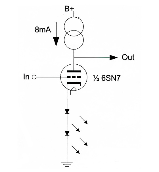
A 6SN7 in grounded-cathode mode with an 8mA constant-current source plate load will show less than 0.04% THD at 20V peak; selected samples will show even less. This distortion is overwhelmingly second harmonic. At 2.83V RMS out, the THD is better than 0.01%, again predominantly second-order. Not bad for a single device, open loop!
Biasing in common-cathode voltage amplifiers typically involves a series resistor in the cathode circuit, with the cathode bypassed to ground. A high-quality bypass cap is bulky and expensive, so an interesting and very viable alternative is the use of forward-biased diodes for developing a constant voltage at the cathode. LEDs are particularly suitable because of their low source impedance, low noise, and reasonably high forward voltage drop. A cheap surplus red LED will typically show 1.7V drop with an AC impedance of 5Ω or less at 10mA current. And it has the side benefit of visually indicating that the tube is indeed drawing current.
Looking at the characteristic curves for the 6SN7, you see that for 8mA of plate current and 160V on the plate, the grid must be about -3.5V with respect to the cathode. Or the cathode can be 3.5V positive with respect to the grid. So two red 1.7V LEDs in series between cathode and ground will automatically provide about the right bias while maintaining a low (10R) AC impedance.
With constant-current loading of the tube, the current through the LEDs will also be constant (because plate current equals cathode current), so any nonlinearity in the LEDs’ impedance with current is suppressed.
Another bonus of CCS loading of the plate and LED biasing of the cathode is the greatly increased power supply rejection. Any noise on the B+ rail is divided down at the output of the 6SN7 by about the ratio of plate resistance to CCS source impedance.
The low impedance of the LED and the high impedance of the CCS mean that this ratio will be very small. For example, with a 7500Ω plate resistance and a 1000M CCS output impedance, any power supply noise or instability is reduced by over 100dB. That’s a very nice way of removing power supply criticality. The outline of the voltage gain stage is shown in Fig. 4.
One notable feature is the use of an input transformer. In an earlier article, I justified its use in some detail; basically, it provides outstanding common-mode hum immunity and galvanic isolation, while at the same time facilitating either balanced or single-ended drive. A 1:1 unit is appropriate here. The gold standard is the Jensen JT11P-1, which I used in the prototype, but other units from Cinemag, Sowter, and Edcor should work equally well. All of these have very low distortion and excellent bandwidth.
Constant Craving
A very good choice for a constant-current source (CCS) is a cascode, and among cascodes, one of the best performers is a FET cascode. Finding JFETs that will withstand the voltages and currents involved is not trivial. High voltage MOSFETs are plentiful and, in cascode, can make an excellent CCS.
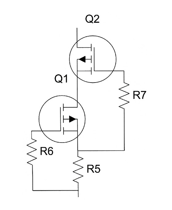
Unfortunately, the biasing arrangements necessary for enhancement mode devices can complicate things. There is relief at hand—depletion-mode MOSFETs are becoming easier to get, and the DN2540 is cheap, available, and works perfectly in this service. A simple yet high-performance CCS using these wonderful devices is shown in Fig. 5. This two-terminal, self-biasing cascode CCS with a source impedance in the 1000M range can withstand 400V without breaking a sweat.
To understand the operation of this cascode CCS, first consider Q1. Its current is set by the value of R5. For a fixed current, the voltage drop across R5 is fixed. Because to first-order the gate current is zero, the drop across R6 (the gate stopper, put there to prevent oscillation) is zero, so Q1’s gate-to-source voltage is fixed at Id times R5.
Considering those flat Id versus Vd FET characteristic curves, that means that the current through the FET is largely independent of the drain-source voltage. If the current tended to rise, the voltage across R5 would rise, which would tend to drive the FET toward lower current. The opposite argument can be made for the FET tending toward lower current. So, because of that feedback effect, Id is constant.
The second FET has a more subtle role. As you modulate signal across the CCS, the drain-source voltage varies. Though the curves are quite flat (i.e., the output resistance is very high), they are not perfectly so. Additionally, the drain source capacitance is significant, especially at low voltages, limiting the source impedance at high frequencies. Worse yet, at lower drain-source voltages, the capacitance is very nonlinear.
Ideally, you would hold Vds constant. And that is the function of Q2, which is connected as a source follower with the gate driven by the source of Q1. R7 is a gate-stopper, as before, with no significant voltage drop across it. Q2’s source follows the signal, so that the voltage between Q1’s drain and source is held constant. Thus, the drain-source capacitance is not modulated, and the constant Vds across Q1 means that current is held more constant—equivalently, you can say that the output impedance is higher.
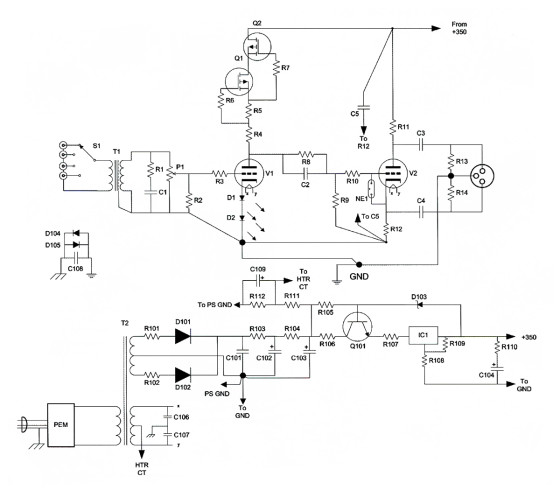
The complete schematic is shown in Fig. 6. You can now start assigning component values. The gate-stoppers’ value is largely non-critical—a few hundred ohms will do. Because I had a bag of 300R carbon resistors, that was my chosen value. If you use 330R or 270R or even 470R, the operation of the CCS will not be affected; it is important to have the body of the resistor as close to the gate as possible. The value of R5 is more critical—that’s what sets the CCS’s current. And the CCS sets the operating current of the voltage amplifier tube.
FETs vary. A lot. It is not unusual to find two devices with the same part number having Idss or gm values that differ by a factor of three. I bought several tubes of the DN2540 and kept one. Those parts were all relatively similar, with two or three outliers from the batch of 100 tested. But I cannot guarantee that other lots of these parts will be so closely controlled. So, although I give the value of R5 that worked for this particular lot, you will need to adjust its value for the devices you have to get the desired operating current.
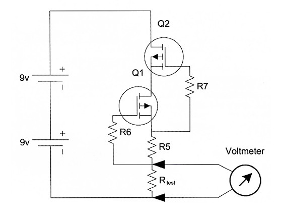
To test the operating current and check whether the initial value of R5 must be raised or lowered, you can use the circuit in Fig. 7. This jig is powered by two standard 9V batteries in series; of course, you can use any other convenient power supply. The current is calculated from the measured voltage across Rtest divided by Rtest’s value. A convenient value is 1k, which will give an 8V drop at the nominal operating current.
Now, the absolute value of the current isn’t extremely critical, but you will need to match both channels. Although 8mA is the design current here, going a little bit higher or lower (say, between 7.5 and 9mA) won’t ruin the performance.
There’s one more little trick up my sleeve—R4. The CCS needs to carry all of the 6SN7’s plate current and drop a lot of volts from the B+ rail (you’ll see later why the B+ rail needs to be fairly high, about 350V). So because the CCS has such a high impedance, adding some series resistance doesn’t much affect its operation, but R4 will dissipate some of the power necessary in the plate circuit. This will eliminate the heat-sinking requirement for Q2, which would otherwise need to remove more than a watt of power. I chose its value to drop about half of the necessary voltage. It serves a more subtle purpose, too—it isolates any of the stray capacitances of the power FETs from the plate circuit. For thermal reasons, it should be generously rated—a 2 or 3W unit is ideal.
Volume controls are a common weak point in analog preamps. You should use a high-quality one; a stepped attenuator would be my first choice. For my prototype, I selected parts on hand wherever possible, so I used an Alps Black Beauty. Personal choice should rule here. A too-large value will interact with the Miller capacitance of the 6SN7 to cause treble losses, and too small can cause loading issues for the input transformer. You need to pick the input circuitry as a team!
You must first and foremost cater to the whims of the prima donna, the input transformer. It is more than a bit fussy about how its secondary is loaded; otherwise, it will make you sorry you ever bought it. And here’s where you’ll need to do a bit of experimenting if you use a different input transformer and want the absolute best performance the pre-amp is capable of. If you use the Jensen, I’ve saved you some time wrestling with scopes and square waves; a 100k control with a 15k resistor shunting it (no capacitor needed) works nearly perfectly.
There is some minor variation depending on the position of the volume control (this is because of the ~80pF Miller input capacitance of the 6SN7), but it is still pretty close to optimal at all positions. For other transformers or other values of volume control, either follow the manufacturer’s recommendation or adjust the values of R1 and C1 using a square wave source.
Out Here In The Fields
With the voltage amplifier stage wrapped up, you can move on to the output stage, which is tasked with taking a single-ended signal and converting it to balanced (the so-called phase splitter), then driving the power amp and associated interconnects.
The ECC88/6DJ8 in the output stage offers a very low source impedance (100R, typical) and it is an easy tube to find in all sorts of flavors. Because of the 100% degeneration in this circuit, there’s little advantage to using any of the collectors’ items in this spot. And other tubes will also work well here—an ECC99, for example, would be a fine choice. I have substituted 7308, 6KN8, and 6922 with no measurable or audible difference. The key virtues are reasonable current capacity and high transconductance.
Now, how do you set up the output stage? In a split-load inverter, the current through cathode and plate resistors is equal, so the voltage drops across them are equal. I want to run the current high enough to keep the tube’s transconductance high, but not so much as to threaten reliability. As with the first stage, 8mA is a good compromise. Now we need to choose the load resistors. Too low and the distortion goes up, too high and it’s difficult-to-impossible to get 8mA of current at any reasonable supply voltage.
Because I’ve used ECC88s in line amps with a 30k load and got reasonably good distortion performance, and 8mA gives a 240V drop (plenty to supply our swing requirements), I will declare that the Official Value. Splitting the load means that the cathode and plate resistors, R11 and R12, are each 15k, with a drop of 120V or so across them at the nominal 8mA. You can now see why the B+ needs to be at 350V or more. R11 and R12 each drop about 120V, and you want 100V or so across the tube to ensure proper operation at the high voltage swings required.
R11 and R12 should be very tightly matched so that the balance and distortion are optimized. If you buy a dozen or two 1% resistors, it should be easy to find a couple of pairs that match to within 0.1%; the absolute value isn’t critical, the relative values are, so the calibration of your ohmmeter isn’t going to be the determining factor in matching.
With the cathode resistor at 120V, the grid will need to be slightly negative of that value, about 118V or so. This presents a small problem — the 6SN7 will likely have 170-180V or more on its plate, so direct coupling becomes difficult. In order to get the output stage grid to the right voltage, you need to lose 40V or so of DC. There are several ways to do this—for the sake of simplicity I used a voltage divider (R8 and R9) with the upper leg bypassed by C2. The voltage divider resistors slightly load the voltage amplifier, but at 1M minimum, the loading is pretty insignificant, more than a hundred times higher than the 6SN7’s plate resistance.
The choice of output coupling caps, C3 and C4, will depend on the expected load; their value sets the bass rolloff corner, with a 3dB down point calculated from f3 = 1/(6.28RC), where R is the expected load resistance. For a 100k load, a very moderate 0u47 capacitor will give an f3 of about 3.5Hz. Although the F4’s stock input resistor is 47k, its value can safely be increased to 100k without worries about offset voltage or RF pickup.
The important thing is to have the input resistors as well matched as possible because they are part of the AC load of the split load inverter. As before, 0.1% matching is easy to achieve by buying more than you need and spending time with an ohmmeter. R13 and R14 hold the output voltage at ground in absence of a load. Their matching is less critical than the lower value load resistors and power amp input resistors. 1% is good enough.
NE-1 serves to limit the grid-to-cathode voltage of the ECC88 at power-up. This is often accomplished by the use of a diode, forward-biased at power-up, but reverse-biased after warm-up. And if a neon bulb is difficult to source, you can use a diode, with its cathode (banded end) connected to the cathode of V2. The advantage of the neon bulb, besides a visual indicator of power-up, is that its capacitance is lower and more linear than a reverse-biased diode. It lights up with a nice orange glow when you first turn on the power switch, then extinguishes as the preamp warms up and the bias LEDs start to light.
Powerhouse
I have endeavored to make this circuit uncritical of the power supply, but it is still worthwhile to try to get to the point of diminishing returns. The huge power supply rejection afforded by the CCS loading of the input stage and the large voltage swings make this a very straightforward exercise. You need a stable 350V for the B+ rail; the constant-current of the voltage amplifier and 100% local degeneration of the output stage go a long way to ease the demands for ultra-low impedance.
Nonetheless, it is easy to make a supply that is orders of magnitude better than what you strictly need for not much more complication and cost than a supply that just does the minimum. So I will don my 16th piece of flair and use an active regulated supply with reasonably low noise and source impedance.
The Maida regulator, based on National Semiconductor’s LM317, has made guest appearances in such designs as Joe Curcio’s Stereo 70 conversion, Morgan Jones’s Crystal Palace, and my own Red Light District. Because of the signal levels involved and the inherent power supply rejection of the signal circuitry, I’ve used a simplified version closer to Curcio’s than Jones’s or the original Maida circuit. If you want to go crazy and add all the extra bypass caps and the protection diodes needed to deal with the consequences, you can boost the regulator’s measured performance, but the sonic effect will be minimal-to-nonexistent. The Maida regulator is easy, low-cost, quite stable, and reliable.
Because the design is discussed thoroughly in Maida’s paper, I won’t rehash it in detail. I used a TIP50A as the pass device, but there’s no reason why any other moderate power transistor wouldn’t work there. A power MOSFET could also usefully serve in that position.
Under operation, assuming a 400V raw supply (a good compromise between headroom and pass transistor dissipation), the regulator needs only to drop 50V, but remembering that the regulator will be turned on and off with the preamp, do not try using a low voltage device for the pass transistor! The regulator draws about 6mA, the signal circuits for a stereo version another 32mA.
So if you estimate the total current to be 40mA, the pass transistor and LM317 dissipate (400 - 350 = 50) volts times 0.040A, or 2W. Most of that is dropped by the pass transistor, so it should have some heatsinking. The output voltage is set by 1.25 times the ratio of R108 to R109. R108 dissipates a bit over 2W, so size it generously. It may be useful to make it from a series or parallel combination of two 2W resistors.
The output capacitor, C104, has a resistor in series with it, basically to flatten out the inductive output impedance of the LM317 regulator. This series resistor means that money spent on an ultra-low ESR cap for C104 is better directed toward booze and gambling. The signal circuitry is locally bypassed by C5.
How do you get the 400V for the raw supply? Looking in the iron pantry, I found a nice power transformer from Allied, the 6K3VG, rated at 650VCT, 40mA. It’s overkill for this job, but it’s reasonably cheap ($25), has a shield layer, and is easy to find. There’s no reason why a surplus unit won’t work just as well. All you ask is that you end up with 400V at reasonably low ripple to feed the regulator. This particular transformer has a conventional E-I core; other constructions will also work—some even better, but avoid toroids. With the universal adoption of compact fluorescent lights and switching supplies, power lines are noisier than ever, and toroids diligently couple that noise into the power supply. High-speed rectifiers are cheap these days, so why not use them?
R101 and R102 keep the ripple currents under control and give the diodes some padding during power-up. I chose the value of C101 to give 400V at the raw supply output; its relatively small value again keeps ripple currents low. This is followed by two RC filters; the ratings of the resistors are reflective of RMS ripple currents. Wirewound resistors are preferred, but the metal oxide type will also do well.
On the primary side, I used a power entry module for the fuse, switching, and IEC line cord plug. You can use individual bits for this, too. Whichever approach you take, make sure that the earth ground lead from the power line is firmly connected to the chassis. Safety is the number one concern! Of the millions of ways of making a raw supply, this is certainly one of them.
As for heaters, the ideal solution is a separate heater transformer so that rectifier noise from the high voltage supply isn’t coupled to the heaters. I took a shortcut and used the 6.3V winding on the power transformer. There is no need for DC here — the signal levels are high, and with some care in layout and lead dress, you can avoid hum. Capacitors C106 and C107 bypass any commonmode noise to chassis ground — they are optimally placed right at the 6SN7 heater pins, though I sited them closer to the transformer. All heater leads should be tightly twisted and dressed close to the chassis, away from any low-level signals.
As is customary, the heater supply center-tap is DC biased above ground, but AC bypassed to ground by C109. This minimizes hum pickup in the 6SN7 and keeps the ECC88 heater-to-cathode voltage within the specified maximum.
We Can Build It, Yes We Can
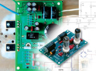
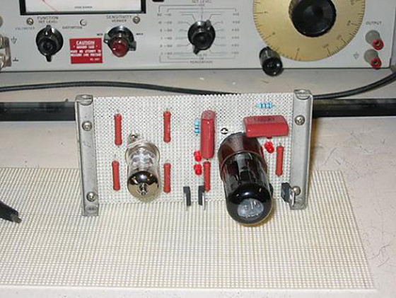
For the prototype, I used a mix of modular boards with different construction techniques. The circuit is simple enough to be done point-to-point or on a perfboard; if there is interest, it would be relatively easy to put the whole thing on a PCB. Photo 1 shows the signal circuitry built on a perfboard. Because of their size, I put the output caps, C3 and C4, on a separate board, positioned between the main signal circuitry board and the output connectors.
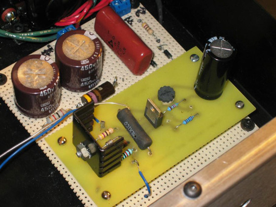
Photo 2 shows the raw supply and regulator, built on a mixed platform of perf and PCB. As is evident, there’s nothing exotic in the componentry, nor (given the pains we took in the circuit design) is there any need. Grounding is straightforward — I used a set of individual stars all brought to a common point, much as indicated on the schematic. The common point is connected to the chassis (safety) ground at one point via a groundbreaker, which helps prevent the formation of ground loops with other equipment.
The groundbreaker is bypassed at RF by C108, whose value is small enough to have negligible conductance at hum frequencies. I found a great source of casework (my own weakness) at DIY Enclosures LLC (update: the company is no longer in business - alternatives exist at diyaudiostore.com and Parts Express). I used their DIY1712 cabinet, which had way more space than I needed. Unfortunately, the inside height is just too small to accommodate the CV1988 and the room needed to clear the pins from the bottom of the case. This is the reason for the vertical mounting of the PCB.
I chose the position so that the tubes were under the vent slots in the case’s cover. I drilled a few holes in the bottom plate to aid circulation, and, as a result, the preamp runs only moderately warm. Output connectors are XLR, just to emphasize the balanced nature. They also look cool and work flawlessly.
On Further Examination
One nifty feature of the split-load inverter is the opportunity to pick off a single-ended signal from the cathode. So if you want to drive an F4 (or other amp) single-ended, you can do so. For the output stage to run as a cathode follower, the plate should be at AC ground. Conveniently, there’s already a capacitor there, C3. So by connecting the output side of C3 to ground, you have bypassed the plate to ground and made a single-ended output available at C4.
This is most easily done by making up a set of interconnects with XLRs at one end and RCA plug at the other. Inside the XLR, wire a jumper between the plate output pin and ground. That way, you can go back and forth between balanced and single-ended just by plugging the appropriate interconnects in and out.
Note that the preamp run single-ended inverts polarity. The test bench performance was all I could hope for. Mid-band THD was 0.04% at 20V peak (40V peak-peak) out into a 10k load, single-ended. This broke down as -68dB second harmonic, -92dB third, and all other harmonics below -100dB. Distortion at 25Hz was slightly worse, with third harmonic measuring -89dB. Hum and noise were below 0.5mV, nearly -100dB from full output.
At 2.83V, frequency response was flat +0/-0.5dB from 5Hz to 48kHz (my test limits). If the 26dB of gain is not an issue, this can serve as a good line amplifier in other installations. But really, it needs to stretch out and swing some volts. It has not escaped my notice that this preamp looks very much like the input stage and phase splitter for a push-pull tube power amp. And there’s no reason not to build a tube unity gain power amp with a balanced input.
Though I have not bench-tested with other 6SN7s, a quick listening test showed that the preamp’s sonics were not degraded by the substitution of a 5692 or a button-base 6SN7GT. Ever in a rush to get things done, the final wiring took place in the back room of the Burning Amp Festival (Photo 3). This occasioned derisive hoots from passersby and curious stares from those who wondered why we’d be soldering instead of doing sensible things like drinking, socializing, and listening to music. Nonetheless, when the preamp was plugged into the balanced F4s, driving a pair of Basszillas, the rush and stress all were worth it — dead silent background and no artificial sweetening or compression.
It did everything sonically that you could want from a preamp, driving the Pass amps without breaking a sweat.
This article was originally published in audioXpress, February 2009.
Erratum: The MOSFETs in the figures are drawn as pFETs, but they are nFETs.
References
1. Morgan Jones, Valve Amplifiers, 3rd Edition, Newnes (2003).
2. Morgan Jones, Building Valve Amplifiers, Newnes (2005).
3. Michael Maida, “High Voltage Adjustable Power Supplies,” National Semiconductor Linear Brief LB47 (1980).
4. Nelson Pass, “First Watt Model F4 Operation and Service Manual” (2006).
5. Stuart Yaniger, “The Heretical Preamplifier,” diy Magazine (2005) (available at www.basaudio.net).
6. Stuart Yaniger, “The Red Light District,” diy Magazine (2006).
7. Joe Curcio, “ST-70 With Solid-State Regulation,” Glass Audio Vol. 1, number 1 (1989).
Acknowledgments
As usual, the gang at diyAudio.com were a great inspiration and help. Mark Cronander really got the project started, and Chris Bridge did far more than a fair share of construction work. I thank Nelson Pass for the use of Fig. 1 and for his support and encouragement, Morgan Jones for his usual perceptive critique (and the CV1988!), and Cynthia Wenslow of Rising Moon Studio and Steve Eddy of Q-Audio for assistance with drawings and organization.
Please visit also the authors website: syclotron.com
Additional reading and Complete Kit by Jack Walton available at TECH-DIY.com
Parts List
Resistors (Signal circuit, two of each needed for stereo)
R1 - 18k, metal film (see text)
R2, R9, R13, R14 - 1M, 0.125W
R3, R10 - 1k, carbon composition, 0.25W
R4 - 12k5, metal film or wirewound, 2W
R5 - 300R, metal film, 0.125W
R6, R7 - 120R, 0.125W
R8 - 680k, 0.5W
R11, R12 - 15k, metal film or wirewound, 1W, matched to 0.1%
Controls
P1 - 100k stereo potentiometer, audio taper
S1 - 2 pole 4 or 5 position rotary switch
Capacitors (Signal circuit, two of each needed for stereo)
C1 - Not used, jumpered (see text)
C2, C5 - 0.1μF, 630V polypropylene
C3, C4 - 0.47μF 400V polypropylene
Semiconductors and lamps (Signal circuit, two of each needed for stereo)
D1, D2 - Red LED, 1.7V
Q1, Q2 - DN2540N5
Depletion mode MOSFET
NE-1 - NE2 neon bulb
Transformer (Signal circuit, two required)
T1 - Jensen JT11P-1 or equivalent 1:1 input transformer
Resistors (Power Supply)
R101, R102 - 47R, 0.5W
R103 - 470R, 3W, wirewound or metal oxide
R104 - 1k, 3W, wirewound or metal oxide
R105 - 20k, 0.5W
R106 - 100R, 0.5W
R107 - 47R, 0.5W
R108 - 56k, 5W, wirewound
R109 - 200R, 0.5W
R110 - 4R7, 0.25W
R111 - 270k, 0.5W
R112 - 47k, 0.5W
Capacitors (Power Supply)
C101 - 1μF 630V polypropylene
C102, C103 - 100μF 450V electrolytic
C104 - 47μF 400V
C105 - Not used
C106, C107, C108 - 0.01μF 600V ceramic disc
C109 - 10μF 100V electrolytic
Semiconductors (Power Supply)
D101, D102, D104, D105 - UF4007 fast recovery rectifiers
D103 - Zener diode, 12V 1W
Q101 - TIP50A or equivalent
IC1 - LM317 adjustable regulator
Transformer and Miscellaneous (Power supply)
T2 - Allied 6K3VG, 650VCT at 40mA, 6.3VCT at 2A
PEM - Power Entry Module, SAE PM1B-6 (included with DIY1712 case)